

Defect of the Month

Exposed copper coupled with silver final finish is causing opens.
Figures 1 and 2 show two images of the same problem: one x-ray, the other optical. In both cases it’s the result of sulphur corrosion on the surface of copper and silver surfaces.
Both surfaces remain exposed after a soldering operation, and in the presence of sulphur, it is possible to witness corrosion. In time it can result in an open connection, as the figures show. Figure 1, taken on a Dage x-ray system, shows different degrees of corrosion on the tracking just below the solder joint fillet. In failure investigations it’s important to see and record as much as possible without change or damage to the sample. On one joint there was an open connection on this QFP device.
It depends not just on where one looks, but when.
Are these open connections, non-reflow or good quality control? It all depends on which stage of the process the product is in when inspected.

One culprit could be package warping.
Figure 1 shows the Amkor TMV package after microsectioning the board assembly during failure analysis. This particular view shows open joints between the top package and the solder spheres on the bottom package.
Poorly maintained baths or improper wave settings can lead to whiskers.
A solder whisker or a dross short is surface contamination found after soldering due either to a poorly maintained solder bath or incorrect setting of a wave. If a solder bath is poorly maintained, dross can be present in the ducting below the solder surface. When the wave operates, any dross can emerge randomly in the wave and contact the board and form micro shorts.
In the case of the back flow on a lambda style wave, the solder should flow at the same speed as the board or slightly faster. The board displaces any surface oxides on the surface of the wave before it can contact the base of the board. If the wave stops flowing before the board exits the wave, the board will contact the surface oxide, leading to what is sometimes referred to as “snail trails.” This can also be seen on waves running nitrogen where only the surrounding areas of the wave are inserted.
Similar micro shorts have been seen during wave soldering in a Pb-free process where the copper level is excessive and the temperature has permitted SnCu needles to form and flow in the wave. The same is true if the surface of the tank becomes eroded, permitting SnCuFe needles in the bath. Both these contamination issues can lead to very fine needle-like solder shorts. The excess copper can be overcome by balancing the copper levels with tin. SnCuFe is a real problem not only to the system but also the extremely expensive alloy, which will need to be changed.
These are typical defects shown in the National Physical Laboratory’s interactive assembly and soldering defects database. The database (http://defectsdatabase.npl.co.uk), available to all this publication’s readers, allows engineers to search and view countless defects and solutions, or to submit defects online. To complement the defect of the month, NPL features the “Defect Video of the Month,” presented online by Bob Willis. This describes over 20 different failure modes, many with video examples of the defect occurring in real time.
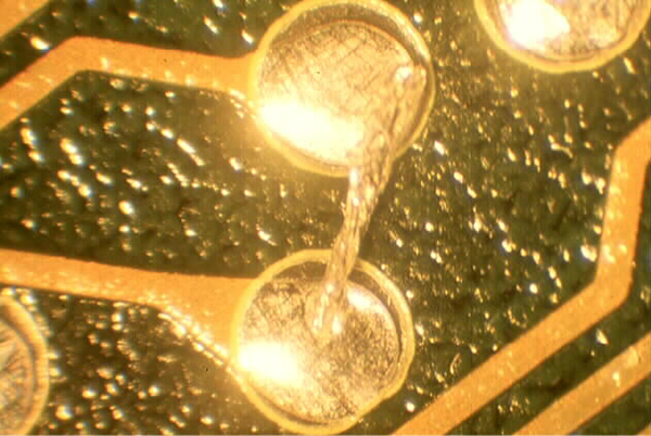
Figure 1. Solder whisker bridging two conductors.
Chris Hunt is with the National Physical Laboratory Industry and Innovation division (npl.co.uk); chris.hunt@npl.co.uk. His column appears monthly.

To avoid extra paste, temper the ball depth.
Figure 1 shows the base of a package-on-package device covered in dip paste. Clearly the package has been dipped to an excessive depth in the paste dip unit. This will be due to incorrect setup of the unit. The bottom of the dip unit, the dip plate, should define the depth of the paste on the balls, and normally should be set to achieve 40% to 50% of the ball depth. There should be suitable process control checks on the dipping unit during production, and the depth of the paste should be measured manually or automatically.
- Other possible causes for excess paste include:
- Component not parallel with dip plate.
- Movement of the component on pickup nozzle during dipping.
- Incorrect depth of paste in dipping unit.
- Package warpage.
- Dipping plate not parallel with component balls.
- Uneven or excess paste in dipping unit.
These are typical defects shown in the National Physical Laboratory’s interactive assembly and soldering defects database. The database (http://defectsdatabase.npl.co.uk), available to all this publication’s readers, allows engineers to search and view countless defects and solutions, or to submit defects online. To complement the defect of the month, NPL features the “Defect Video of the Month,” presented online by Bob Willis. This describes over 20 different failure modes, many with video examples of the defect occurring in real time.
Chris Hunt is with the National Physical Laboratory Industry and Innovation division (npl.co.uk); chris.hunt@npl.co.uk. His column appears monthly.

Press Releases
- Orbit Technologies accelerates growth and doubles production capacity with Europlacer iineo placement machine
- CE3S Brings Back Free ANSI/ESD S20.20 Training Series This August with Desco Industries
- Green Circuits Names Adam Szychowski Chief Revenue Officer
- MicroCare Appoints Doug Kay as Director of Market and New Business Development