

PCB Surface Finishes: When to Change It Up

The primary purpose of surface finishes is to prevent oxidation of the copper prior to soldering components.
Back when I held a soldering iron, we used a mixture of tin (63%) and lead (37%) for the solder (Sn63). The boards had the same coating on the plated holes and surface-mount pads. The application for surface mount is referred to as hot air solder leveling (HASL) and applies to any of the available solder types. The beauty of Sn63 is it has a lower melting point and is eutectic. “Eutectic” means the metal solidifies rapidly over a short temperature range. The benefit is fewer disturbed solder joints and good “wetting,” where the surface finish and the solder form a cohesive bond for a reliable connection. You can still buy Sn63 off the shelf at the local electronics store.
On the other hand, lead is a dangerous metal that can cause birth defects and other health issues. The Europeans took the vanguard with the RoHS initiative. If you want to sell electronics products to consumers, the lead content must be the minimum possible – not eliminated entirely but found primarily as a trace element within chips.
SAC (Sn-Ag-Cu): a heroic alloy. Metallurgists all over the world looked for replacement formulas. Tin is still viable and is generally mixed with small amounts of silver and other elements such as antimony, copper or bismuth. Tin makes up the bulk of the alloy, typically around 95% to 99.3%. If pure tin was used, the results could be problematic. Tin whiskers from dendritic growth present a shorting risk.
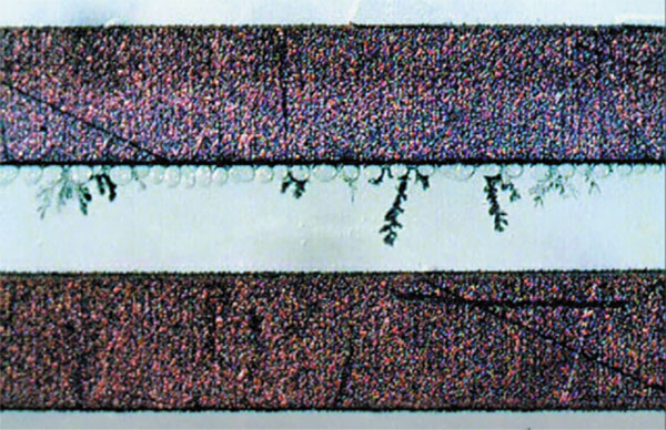
FIGURE 1. Pure, non-alloyed metals exhibit crystalline growth as the metal forms branches over time. Environmental conditions can aggravate the process. (Source: NTS Corp.)
Without lead, tin has a much higher melting point and does not solidify as quickly. The double-complication requires a dielectric material that can withstand the higher temperatures without breaking down.
The maximum working temperature of the material is one of the primary selling points. It is known as the glass transition (Tg) temperature. The materials we used in the old days did not stand up to the process, so the entire PCB material set had to be seriously upgraded. Going lead-free raised the reflow temperatures considerably. Boards and components alike have gone green since then.
Exemptions exist where tin-lead is still allowed. Spacecrafts that will eventually burn up on reentry are one such exemption. The goal of RoHS is to reduce the amount of lead that goes into the landfill. Provided the company can certify all its products will be returned to the factory for proper disposal, Sn63 coatings on the PCB are permissible. Obviously, consumer products do not get such an exemption.
ENIG: the gold standard. While tin-silver plating is still viable, the “gold standard” is gold. The mainstream alloy is immersion gold over electroless nickel over copper, or ENIG for short. The reason this is a preferred plating is the downstream process of assembly is more boring without the likelihood of tin whiskers. We like it to be boring when it comes to making goods. Those who study S-parameters also have a fondness for the consistency of ENIG finishes.
This plating is primarily aimed at high-density interconnect fabricators. The process can yield a solderable footprint with via-in-pad situations. Fine-pitch BGAs and other shrunken circuits require microvias. Plating with ENIG will likely improve yields due to the land patterns coming out flatter than with other types of plating. It’s also a go-to finish for flex circuits. It plays well with solder mask, making a good base for the following layer.
FIGURE 2. ENIG finish with through-hole vias and surface-mount components.
A note on “black pad”: This process defect was a hot topic for a few years. That time has passed. The fabricators worked out the right amount of phosphorus in the nickel to prevent the defect that was more than a cosmetic issue. That concern was laid to rest.
ENIPIG: not too hard, not too soft. Electroless nickel, immersion palladium, immersion gold adds palladium as a physical barrier between nickel and gold. That opens up the process. The main benefit to ENIPIG is the outer layer of gold is soft enough to be a good candidate for wire bonding, while still working well for soldering. The alternative for chip-on-board is a selective soft gold finish: the do-everything finish.
When selecting the correct finish, know the constraints. While ENIPIG has an upcharge, it’s not as expensive as soft gold or hard gold when used in combination with medium gold. Note medium hardness is geared for solderability, while hard gold creates a more durable contact surface for “gold finger” edge connectors. To meet the specification for HDMI, the gold fingers must withstand 10,000 insertion/extraction cycles.
OSP: a minimalist approach. Organic solderability protectant is a very thin coating consumed by the reflow process. In the factory, we had to be aware of the date codes on boards with OSP. You don’t want old boards with this coating.
During design, when reaching back to padstack definitions, the designer must coordinate something extra when using OSP. We had to include a paste stencil opening on our test points when the boards had OSP, or the test points would end up with bare copper. The exposed copper will tarnish over time. None of the other finishes have this requirement.
An IPC specification for OSP (IPC-4555) is on the horizon. Per a report on this publication’s website in August 2020, “The goal is to develop performance specifications for high-temperature OSPs, defined as capable of withstanding up to two IR reflows in conjunction with tin-silver-copper (SAC) or tin-bismuth (SnBi) alloys at a peak temperature of 245°-250°C and showing the same wetting balance results at three reflows as zero, with a maximum 20% drop.”
This is good news since OSP is well-suited to mass production runs. The micro-thin coating does not hinder solderability. The cost is low, along with the shelf-life. Organic solderability protectant has been around for quite some time with proprietary processes, so it will be beneficial to have a performance standard across the board.
is a career PCB designer experienced in military, telecom, consumer hardware and, lately, the automotive industry. Originally, he was an RF specialist but is compelled to flip the bit now and then to fill the need for high-speed digital design. He enjoys playing bass and racing bikes when he's not writing about or performing PCB layout. His column is produced by Cadence Design Systems and runs monthly.


Press Releases
- Altus Adds LPKF CuttingMaster 3290 to Depaneling Portfolio
- Kurtz Ersa Partners with E-tronix for Sales in Illinois and Wisconsin
- XLR8 EMS Welcomes Raul Jorge Lopez Jr. as Director of Program Management and Procurement
- Koh Young America Promotes Ramiro Mora to Lead Service and Applications in Mexico and South America