

Preparing a PCBA for Harsh Environments

Shake, rattle and roll: Your devices often experience it all.
The stark choices of organisms are to adapt, move or die. Our electronics sometimes tough it out so we can do our jobs or simply have a good romp on our favorite ride. No matter the purpose, extreme weather puts an electrical system to the test.
Whether the element is sand, saltwater, sunshine or perhaps a lack of thereof, many dangers age a system prematurely. Most faults caused by the environment are single-component failures. Okay, a part failed. Why? What is the root cause, and what can we do to prevent it from becoming part of a larger trend? Answering that two-part question is the gist of reliability engineering.
What broke is not always evident. Cosmetic damage or a burn scar may point the way if you’re lucky. In most cases, diagnosis is not that easy. Check connectors first, while the board-level investigation usually centers around the FETs that bring power to the device that is out of spec or failing altogether. Somewhere in there a tiny junction has burned up. The repair and return unit or perhaps field service technicians are a good source of reliability anecdotes.
Shock and vibration over time will make anything rattle itself to pieces. We can run into unexpected issues with resonant frequencies. Remember the footage of the Tacoma Narrows Bridge. “Galloping Gertie” came down, as the roadway itself was wind-tossed into 30' waves. The same thing happens on a smaller scale and at higher frequencies all around us. Something will begin to rattle in the wind until it breaks off.
Spread out components to relieve heat buildup. What separates high-reliability PCB footprints from standard ones? You’ll see the difference in the size of the solder pads. Expect more room for the toe fillet. This often increases the personal space around the component, while providing additional metal-to-air interface area for convective heat dissipation. The additional spacing created by the extra metal may not seem like much, but on aggregate has been shown to reduce junction temperatures.
Derating for system robustness. The other thing that separates high-reliability footprints is simple. Stuff them with components that are better than good enough. Twice as good is a high bar, and a good place to start when it comes to derating components. If a 50V cap is sufficient, go for the 100V version.
Chunky hardware with closer spacing isn’t just for the steampunk effect. Plan a few mounting holes in the middle of the board, rather than just the corners. You’ve seen a heat map. The hot spot isn’t on the edges. As a practical matter, a gratuitous hole here or there could be a bargaining chip as the board evolves into something more crowded than originally planned. You know what they say about plans.
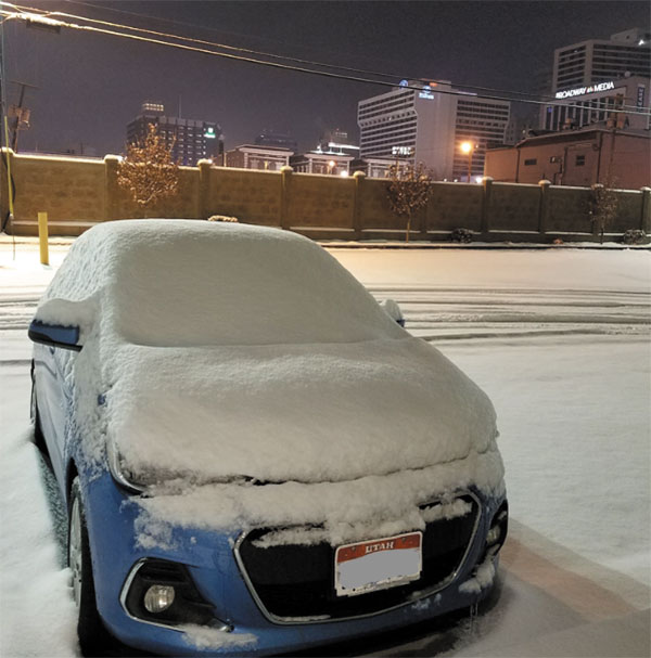
FIGURE 1. While this overnight accumulation looks tame to some, moisture is an archenemy of electronics (and other metal objects).
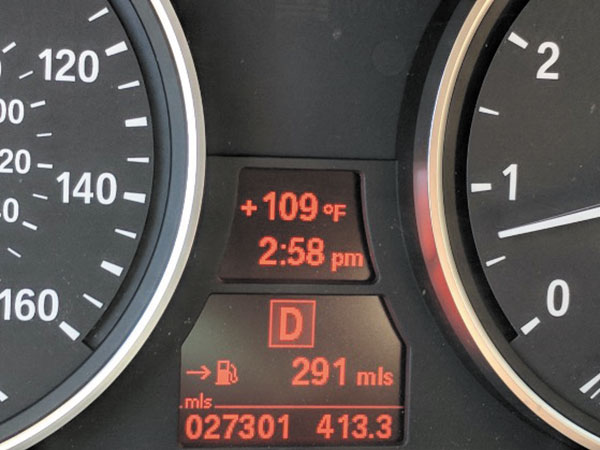
FIGURE 2. The car suffers in the midday sun, and I come along and demand it envelop me in a cocoon of frigid air. Like it or not, that’s hard on the equipment.
Commercial- versus industrial-grade components. It was easy to distinguish the TTL packages of yesteryear. The high-reliability units had a device number “54,” rather than the “74” used on commercial versions (FIGURE 3). LS stands for low-power Schottky, which predates the even lower-power CMOS architecture. This example is a stand-in for the universe of components that follow this technology path.
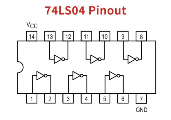
FIGURE 3. This hex inverter circuit plays out on different footprints, starting with DIP packages, and then SOIC became the surface mount version for the plastic package. The underlying silicon underwent several iterations, and the high-reliability versions are on their own package outlines. (Source: Netsonic)
Operating ambient temperature range and package comparison:
54 = -55°C min., 125°C max. Packages: CDIP, LCCC, CFP
74 = 0°C min., 70°C max. Packages: PDIP, SOIC
Ceramic packages withstand a greater range of temperatures than plastic ones. No surprise high-reliability packages are not always the smallest available. It’s a paradigm that carries through connectors down to passives. Get those commits early and nurture them so the part pipeline is there when you need it. Mil-spec parts are an upgrade whether the board is Class 3 or Class II commercial, so it’s about cost and availability.
Use adhesives and conformal coatings to prevent unintentional disassembly. For everything to stay put, a shaker table will be part of your life. These instruments of mechanical terror are specially designed to shake other smaller things to the point of failure. You can only imagine how overbuilt a shaker table must be to outlast whatever is bolted down on its base plate.
When the dust settles, the weakest link(s) will be revealed, and additional actions can be taken. During the preproduction trials on the Pixel laptop, we had a connector that would not stay put after the 3' drop test. We hope you never give your laptop a 3' drop onto concrete, but if you do, a little bracket holds the USB connector in place.
Riding around on the roof of a car is another challenge you should never have to face. Putting a Lidar detector up there, on the other hand, can be loads of fun (FIGURE 4). Simultaneous location and mapping (with the somewhat unfortunate acronym SLAM) require an immense amount of processing while jostling around through rain and sleet. The connectors, in particular, are well overbuilt, especially when you’re looking for a place to put that ethernet port. Nonetheless, a bead of glue around the base is an insurance policy. Post-assembly coatings make rework next to impossible but also protect the devices from failure, making it a good idea for space-bound projects.

FIGURE 4. A car roof is a good place to be out in the elements. Any outdoor location will do, while motion will amplify the effects.
Use heavier copper to give the boards some backbone. Not sure if anyone besides those in the PCB industry use copper weight as the significant variable to determine its thickness, but here we are. Take 1 oz. of copper, keeping in mind it is very malleable, and shape it into a 1' square of even thickness. That’s 1 oz. copper and typically about as much as would be used for the outer layers, while the innerlayers typically get half that.
Both inner- and outer layers can be plated up. One result of this is an increase in the minimum trace width and spacing geometry. The thicker the copper, the coarser the line-to-line pitch becomes. At the extreme, an entire base plate of copper with no circuit pattern can be incorporated into a board. That could be a solid copper bottom layer or as a central metal core. For a local effect, a so-called coin can be embedded as an integral heat sink.
Shock mount electronics inside a cage within a cage. Flight cases offer a standard 19" equipment rack-mount isolated from a secondary outer case that ensures the contents are not subjected to sudden g-forces from being loaded and transported. Something is better than nothing when it comes to bolstering the unit against the expected use-case.
Depending on where you want to go and what you want to do, your electronics must be hardened against failure. We are often the cause. Who hasn’t dropped their phone? The reliability lab focuses on finding root causes of failure. Take whatever measures are necessary and prudent for the perils the gear is likely to face.
Sometimes, reparability will suffer for the effort of making it bulletproof. The motivation is to reduce or eliminate repairs in the first place. Fail fast and go to mass production with the most solid product you can put out there. Your customers will then put it to the test so you can continue the cycle of continuous improvement.
is a career PCB designer experienced in military, telecom, consumer hardware and, lately, the automotive industry. Originally, he was an RF specialist but is compelled to flip the bit now and then to fill the need for high-speed digital design. He enjoys playing bass and racing bikes when he's not writing about or performing PCB layout. His column is produced by Cadence Design Systems and runs monthly.


Press Releases
- Altus Adds LPKF CuttingMaster 3290 to Depaneling Portfolio
- Kurtz Ersa Partners with E-tronix for Sales in Illinois and Wisconsin
- XLR8 EMS Welcomes Raul Jorge Lopez Jr. as Director of Program Management and Procurement
- Koh Young America Promotes Ramiro Mora to Lead Service and Applications in Mexico and South America