

Wrong Steps: How Your PCB Footprints Could Be Holding You Back
 A good library is built with an understanding of the manufacturing limits.
One of the primary factors in the quality of a printed circuit board design system is the makeup of the component footprints. The board can only be as good as the foundational pieces. Making it up as you go along is not a process for the long term. Errors or inconsistencies in the library account for a fair share of the feedback we receive from the fabricator. That is the wrong time to consider the fundamental building blocks of our collective occupation.
The source of the component footprints should be considered. A good cross-section of the supply chain provides the customer with schematic and layout symbols. This is, of course, to make it easier for us to implement their chips and other parts. CAD tools often come preloaded with a number of device examples to get you started.
Take those "freebies" with a grain of salt. One of the ways this kind of help can get in the way is in terms of traceability. One of the more important aspects of a good library is to have one and only one instance of a particular part. Naming conventions come into play here. Many, but not all, of the baseline libraries use naming conventions outlined by IPC-7351.
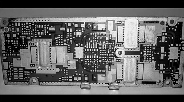
Figure 1. A vendor display case at a trade show had a copy of a Spectrian PCB it did for us. (I had called five meetings discussing the board prior to tape-out as we were doing something entirely new. Dr. Crescenzi included me in the patent regarding the rows of plugged vias along the edge of the slots. Those have a counterbore and fill process to create ground vias from layers 2-4 where layer 4 is a 1mm-thick copper slug.)
Before incorporating any new files, compare the existing name to the one derived from the specification and part geometry. The goal is a level of traceability and repeatability such that you can find it in your library, if it exists. That way, you won't create and maintain one you didn't need.
IPC divides component footprints into three classes just as it does with bare circuit boards. Whenever appropriate, I choose Class 3. These are the high-reliability versions with larger SMD pads. The pads mainly extend on the toe-fillet side, outward from the part. These maximum material condition (MMC) layouts dissipate more heat per pin and create more distance between components. This might be applied selectively in problem areas such as power supplies.
While board space grows, the overall effect is longer component life over normal or high-density classes. Probe access for testing improves, silkscreen marking is more distinct and, finally, rework is improved with fewer lifted pads. Improve product quality with the country living. Using these symbols does not in itself make the bare PCB a Class 3 board, but it is one of the conditions to be met.
There is a corollary with going smaller than "nominal" dimensions for your components. The undersized footprints are useful in RF applications where the SMD pad creates an impedance mismatch, as it differs from the transmission line. The assembler will be happier with all the footprints of the same type. As far as I've noticed, nominal footprints are the mainstream choice for telecom and enterprise. Outside of the cellphone ecosystem, I have not seen much call for MMC.
Footprint library creation. The folks at Ultra Librarian or PCB Libraries could probably tell you more. These outfits compete in the Library as a Service segment. These are not the only players, but they are well-recognized in the ECAD industry. The services break down to an individual bill of materials or some form of subscription that fits your run rate on new PCB footprints.
Circling back to naming conventions, it is next to impossible to cover every conceivable permutation that surrounds a part (FIGURE 2). We start with the general terms of the geometry and work from there. The general code for the BGA package is as follows:
BGA + Pin Qty + C or N + Pitch P + Ball Columns X Ball Rows _ Body Length X Body Width X Height.
Which leads us to the following footprint name for the package in Figure 2: BGA35C40P5X8_ 356X270X050. A few modifiers can be added as a suffix such as when pin A1 is in a different corner. The name alone, in this case, is sufficient information to create the footprint.
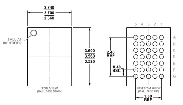
Figure 2. From this image we can derive a unique file name. The package name itself is sufficient data to generate the footprint. Other symbols are more complex and may be categorized by function or by vendor. Source: Analog Devices
Other cases may arise where some random pads are deleted and you find it next to impossible to fully describe the footprint within the available parameters. The IPC has a work-around. When a vendor chooses its own route outside of the established form factors, we use that vendor's name and their internal part number. Figure 1 shows a trio of sockets for amplifiers that require a controlled depth slot along with the pads on the wings. There's just no comparison.
Just about every surface mount connector falls into the same gap where there is no standard footprint. It's as if they all go out of their way to be a little different to each other so that their parts are harder to replace with other brands once they've won the socket. Another thing that seems common among connector vendors is to use really tight tolerances on certain elements, especially alignment hole position and size tolerances.
Question the data sheet. In the early days of the USB-C connector rollout – about a decade back – I captured all the details of the USB connector including the hole and slot tolerances. The connector vendors had not thought to move the alignment hole and slot inboard away from the surface mount pins. With the proximity and miniscule tolerances, the fabricator balked at the fab drawing and artwork that included the intricate geometry. Many of the connector spec sheets are still ahead of the manufacturability curve.
One thing you don't want out of your printed circuit board is a DfM comment from the vendor suggesting that you shave a few SMD pins and open up the non-plated hole/slot tolerance. I didn't think that one through when I was including those values in the library part. Ensure your component vendor isn't too conservative with the source control drawing (FIGURE 3).
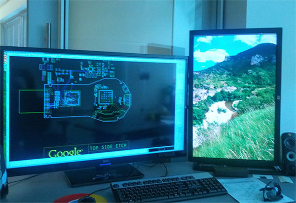
Figure 3. The good old days circa 2014 when one of my boards was the original Chromecast. I had to adjust Google's expectations in terms of placement density. A lot of Wi-Fi dongles plus years with Qualcomm had calibrated my placement norms. They basically had data centers motivating the library, so we upgraded from max to min on spacing.
Fortunately for me, the fabricator was a subsidiary of the original design manufacturer (ODM), and I was able to insist it deliver a finished assembly that meets the requirements for the laptop notwithstanding any fabrication issues. All I needed to know was the end solution so I could incorporate those values going forward with any other boards. Best shop practice became the standard for us.
Solder mask: the linchpin between fabrication and assembly. If your naming is traceable and the geometry is acceptable to fabrication and assembly, you're on the right track. The solder mask layer is a primary concern to both fab and assembly, so don't sleep on the definition of these openings. A smooth edge is necessary for a good mask adhesion. Solder mask slivers arise when we expand the mask when it should have been contracted instead. Most component vendors prefer expanded mask. The 0.4mm pitch of Figure 1 is as fine as you can go with solder mask-defined lands.
At 0.35mm pitch on a BGA device, you're better off going with a metal pad that is 0.25mm diameter with a mask opening of 0.20mm, or something close to this. The non-solder mask-defined land accommodates the microvia-in-pad necessary for this type of device. No routing solution runs a trace between pads on anything less than a 0.5mm pitch BGA. A good library is built with an understanding of the manufacturing limits.
You still must set priorities in terms of what will be in the silkscreen. The must-have is any polarity or pin-one marks for diodes and the like. Second is the reference designator, followed by the part outline, which should be reserved for substantial components like the IC and connector types.
The library is not complete until it has been through a full cycle of product enablement. By then, a cohesive style should be in place for the details. Creating how-to documents when you get it all shaped up pays it forward to those who will be taking the mantle of librarian down the road somewhere. The job is never done.
is a career PCB designer experienced in military, telecom, consumer hardware and, lately, the automotive industry. Originally, he was an RF specialist but is compelled to flip the bit now and then to fill the need for high-speed digital design. He enjoys playing bass and racing bikes when he's not writing about or performing PCB layout. His column is produced by Cadence Design Systems and runs monthly.


Press Releases
- Altus Adds LPKF CuttingMaster 3290 to Depaneling Portfolio
- Kurtz Ersa Partners with E-tronix for Sales in Illinois and Wisconsin
- XLR8 EMS Welcomes Raul Jorge Lopez Jr. as Director of Program Management and Procurement
- Koh Young America Promotes Ramiro Mora to Lead Service and Applications in Mexico and South America