

Expanding Coverage with Boundary Scan
Boundary scan is the present and the future. Are you ready?
Boundary scan has been widely adopted to maintain test coverage and board quality.
More commonly used in boards for telecommunications, high-end servers and high node count boards with limited test access, boundary scan provides not only a means of structural test for complex devices without the need to understand its core logic, but also to address a loss of test access.
With more test methods evolving from boundary scan, one can now expect boundary scan to provide test coverage beyond just boundary scan devices. Test coverage can now expand to the components connected to or in between boundary scan devices on the circuit board. This incremental test coverage can be achieved without adding physical test access to the existing board.
Some of the test methods developed through the evolution of boundary scan include DriveThru (series components) in Interconnect test, virtual test (commonly known as silicon nails test in the in-circuit test world), and powered vectorless test.
DriveThru in interconnect test. Boundary scan interconnect test can be applied on a board where two or more boundary scan devices are connected up in a chain. During the test, the interconnecting nodes between boundary-scan devices will be exercised and tested. In typical board designs, components like resistors or AC-coupling capacitors may be loaded in series along the interconnect nodes (Figure 1).
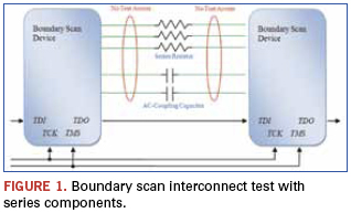
In this situation, these series components can be tested during boundary scan interconnect test as signals are driven through them. Although it does not test for the series components’ value (in terms of resistance or capacitance), it does provide manufacturing defect coverage like presence, opens, shorts, and even shorted-capacitor for AC-coupling capacitor in a 1149.6 interconnect test. Without DriveThru in boundary scan interconnect test, this additional test coverage would not have been possible, unless physical test access were available on the interconnect nodes.
Virtual test (silicon nails test). Silicon nails is a test methodology that tests a non-boundary scan IC device (e.g., logic gate, buffer, memory) through a boundary scan device or chain. A valid test library for the non-boundary scan device is required before silicon nails can be generated. On some test equipment, the necessary test patterns for testing the non-boundary scan device can be automatically embedded into the boundary scan test patterns. An example of how the test signals are passed between the components is shown in Figure 2. The first boundary scan device will output a "00" into the two inputs of the AND gate and subsequently clock in the output response from the AND gate into the second boundary scan device. The next set of input patterns “01” will then be driven and so on.
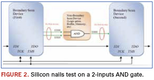
Depending on the test library and circuit topology, the non-boundary scan device can be tested completely by executing a silicon nails test with full input permutation. Compared to a standard digital test, silicon nails can provide the same level of coverage, with same fault diagnostics capability down to the pin level, and yet feasible in situations where direct test access is not available.
In situations where series resistors are connected between the boundary scan and non-boundary scan devices and the test access is not available on these nodes, silicon nails are able to drive signals through the series resistors, thus ensuring their presence while testing the non-boundary scan device. This improves the test coverage as it includes the presence test for the series resistors.
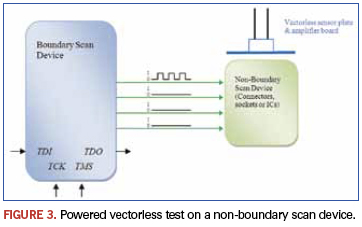
Powered vectorless test. Powered vectorless test is a test methodology using both boundary scan and vectorless test methods. The boundary scan device will drive input stimulus to the non-boundary scan device (connectors, sockets or ICs) and subsequently pick up the coupling signals via a sensor plate (Figure 3). The whole concept is similar to the conventional unpowered vectorless test, except that now the input stimulus is driven by the powered up boundary scan device.
A significant amount of test access is lost as use of surface-mount connectors increases. Previously available test access from through-hole connectors is gone. There is also a large amount of test access on high-speed signaling paths that are removed to improve signal integrity. This has challenged the application of manufacturing test. Powered vectorless test has proved viable in such situations, where previously it would have been impossible to cover such test requirements.
Conclusion
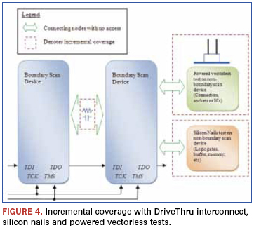
Do not underestimate the potential of boundary scan. The extent of coverage that boundary scan test can provide goes way beyond the boundary scan device itself, far exceeding what one would have thought possible (Figure 4). Incremental coverage on series components with DriveThru in interconnect test, digital-like coverage on non-boundary scan ICs with silicon nails test, vectorless-like coverage on connectors, sockets and non-boundary scan ICs with powered vectorless tests bring board test coverage to a whole new level.
What I have discussed is only the tip of the boundary scan iceberg. Other test methodologies include in-system programming (ISP), built-in self test (BIST), pull-up/pull-down test, new IEEE P1687 standard, and many more. For boundary scan to be successfully implemented, the whole supply chain must be inclined toward it. Whether IC designer, board designer, layout designer, ICT test developer or even repair operator, everyone plays a part in making the whole test suite succeed.
Tan Beng Chye is a technical marketing engineer with Agilent Technologies’ (agilent.com) Measurement Systems Division; bengchye_tan@agilent.com.


Press Releases
- Seika Machinery’s SMI 2026 Webinar Series Continues with Focus on PCB Cleaning Before Solder Paste Printing
- Forwessun Expands Testing Capabilities through Strategic TRI Alliance
- Federal Electronics Expands Advanced Manufacturing Capabilities to Support Military and Aerospace Cable Assembly and Wire Harness Programs
- Altus Continues Irish Growth with Expansion of Engineering Team