

How to Build a Batch of 12-Layer PCBs in 72 Hours

An hour-by-hour look at the quickturn fabrication process.
We were presented with a challenge: Is it possible to build 10 prototype 12-layer boards in 72 hours? It wasn’t a rhetorical question; a customer really wanted just such an order. So, with time at a premium, our engineers put their heads together and created a “plan of attack” that optimized all resources. One key to success is performing a number of the steps in sequence as needed, so panels are ready when they are required. We’ll describe the procedure hour-by-hour as follows:
Hour 1: The CAM operator runs a DRC (design rule check) process and accepts or rejects the data files. If a problem exists, they contact the buyer to work out a solution; e.g., if two traces are too close, and one needs to be moved. Once the data file is accepted, the next action is to set up the innerlayers.
Hour 3: The innerlayer part of the multilayer in CAM is set up first. This will start the process before procedures like drilling or solder mask, which are not required yet. The CAM operator will scale up the innerlayers, so after etching they are all the same size. Since the innerlayers contain different dimensions of copper area, the copper and initial lamination procedure locks in stresses. Once the copper is etched off, the laminate is free to relax and stretch back, changing the size of the panel. Between the smallest change – i.e., a double-sided copper full ground plane and an innerlayer with only a few thin traces – there can be up to 18 mils of length difference between innerlayer panels over 24" to account for. Once panelizing and processing the data for the innerlayers is finished, the CAM operator is free to work on the rest of the manufacturing package, while the innerlayers are processed.
Hour 5: The thin innerlayer laminate is removed from stock, tooling holes punched, the panels cleaned and dry-film laminated.
Hour 7: After imaging, the panels are developed and etched. If the PCB facility has an LDI, the files will be ready by the time the innerlayer panels arrive dry-filmed. If not, the photoplotter will be plotting the innerlayers during hours 2 and 3, so they will be ready when the innerlayer panels arrive for imaging.
Hour 8: Once an AOI (automatic optical inspection) unit inspects the innerlayers, they are punched with the optical lamination pinholes. This ensures the innerlayers are properly registered (line up) with each other in the press.
Hour 10: The innerlayers head to hot press lamination for layup in a press book for lamination.
Hour 11: The actual hot press lamination and cooldown runs for 5 to 6 hr. In the meantime, the CAM operator completes the rest of the images and creates solder mask and white marking programs. The CAM operator also creates a drill-and-route program and finally an electrical test software routine or program.
Hour 18: The panels are removed from the cooldown press; the edges are trimmed, and the panel is sent to the x-ray alignment drill. This machine looks inside the panel and chooses the best location for the drill tooling holes and adjusts the drilling software to the size of the panel.
Hour 20: Due to heat, the process of lamination changes the overall dimensions of the panel by as much as 15 mils. This needs to be measured and adjusted. The x-ray alignment machine will send a file with each panel to the drill to change its program size to more accurately hit the centers of the innerlayer pads.
Hour 22: Boards are pinned, attached to the drill bed, centered and the through-holes drilled.
Hour 23: The panels are deburred, cleaned and dried in an oven in preparation for electroless copper application.
Hour 25: The panels are processed on the electroless line or through a conductive polymer spray machine.
Hour 28: The panels head to cleaning and dry-film application.
Hour 30: After dry-film, the image is exposed to UV light using a phototool or shot with an LDI.
Hour 32: After exposure, the panels are run through the developer.
Hour 34: The panels are copper-plated, and a thin layer of tin is applied as an etch resist.
Hour 39: The panels head to dry-film removal and are processed through a copper etcher to remove the outer layer of excess copper that is not protected by the tin coating. The tin is removed in a conveyorized machine.
Hour 44: Panels undergo AOI. If shorts are present, a laser ablates them.
Hour 48: Once the outer layers are inspected and passed, the panel heads to solder mask, which can be a silkscreen operation or applied by inkjet machines. After exposure and developing, the next stage is solder mask curing, either in an oven or through a UV machine.
Hour 53: The final finish is applied either by ENIG or hot-air-leveled tin.
Hour 56: The panels are sent to electrical test to be tested for shorts or opens, typically on a flying probe. If required, the coupon is impedance-tested.
Hour 60: Once electrical test is passed, the panels proceed to white marking, either by silkscreen application or inkjet spray to apply the markings.
Hour 62: Each individual PCB is routed, as required.
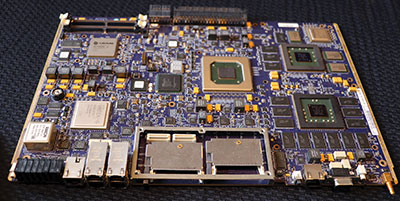
Figure 1. Sequential processing aids quick turns.
Hour 64: Quality Control checks the boards for overall size, ensuring hole dimensions are correct and within tolerance and the overall quality of the board and solder mask are acceptable.
Hour 69: The boards are vacuum-packed and boxed, ready to be shipped.
Hour 71: Ten 12-layer PCBs are finished, with one hour to spare. In the meantime, between processes after etching and solder mask, coupons are punched out, and the laboratory cross-sections them and performs tests to ensure no cracking of hole corners and the correct amount of copper plating was applied. The cross-section will also allow inspection of innerlayer alignment. If all is well, the finished boards ship to the customer.
is chief executive officer of Rush PCB Inc., a printed circuit design, fabrication and assembly company (rushpcb.com); roy@rushpcb.com.


