

10-Layer High Density Interconnect Board Design
 A primer on the steps for building advanced PCBs.
To get more functionality out of boards but within the same or reduced board sizes or areas, OEMs are increasing the density of the product by means of high density interconnect (HDI) boards, which are PCBs with multiple layers vertically connected with blind or buried vias.
HDI PCBs use high-performance thin materials, and have fine copper lines and microvias. While various methods are available, some patented, some not, we use what’s known as Every Layer Interconnect (ELIC) technology, which produces very thin flexible PCBs with high functional density per unit area. Advanced HDI PCBs make use of multiple layers of copper-filled stacked in-pad microvias that enable interconnections with even greater complexity.
One such board we recently built was a 10-layer PCB with FR-4 grade prepreg (TUC-872SLKSP), beginning with all layers of 1/3 oz. copper. The outer layers of copper were coated with electroless nickel immersion gold (ENIG), and covered with a coverlay (green mask) of thickness 0.0249" ±0.003". Component placement was aided by a printed white silkscreen, while the width and spacing of copper traces in each layer were calculated to give precise control of impedance. The board has an overall size of 6.857" x 5.287".
Stackup design. Before finalizing the design of multilayer PCBs, designers need to confirm the structure of the board primarily based on the scale, physical
size, and electromagnetic compatibility (EMC) requirements. Considering the above, our designers decided to use 10 layers of material, and have decided the placement of the innerlayer and the manner of distribution of different signals in these layers, i.e., the stackup design of the multilayer PCB. Careful planning and determination of the stackup design beforehand will save much time and effort in wiring and production later.
Once the designers have determined the number of layers, two key decisions must be made: distribution of the special signal layers and distribution of power and ground layers. With multilayer boards such as this one, our designers follow some general principles to obtain the best combination of signal, ground and power layers:
- Signal layers are kept next to an internal power or ground layer, shielded by the copper film of the internal power layer;
- To maintain tight control over impedance, internal power layers are integrated tightly with the ground layer, so the thickness of the prepreg between the internal power and ground layers is kept thin, on the order of 2 mils;
- No two signal layers are located adjacent to one another, to minimize crosstalk. A ground layer is placed between two signal layers to avoid crosstalk;
- Multiple grounded internal power layers are used to control ground impedance;
- The layer structure is designed to be symmetrical.
The final stackup is shown in FIGURE 1. The overall PCB thickness is 27.20 mils, or 0.69mm.
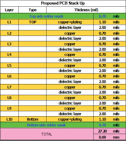
Figure 1. Final stackup.
ELIC. To achieve very high-density interconnection, we use Every Layer Interconnect Technology. With ELIC, each layer has its own copper-filled, laser-drilled microvias. When stacked, it provides the opportunity for dynamic connections between any two layers in the PCB. Not only does this offer an increased level of flexibility, but it also maximizes circuit density. The designers took on the added challenges of routing with via-in-pad (VIP) and employing blind and buried vias. Vias were drilled with lasers and filled with conductive copper paste. In our sample 10-layer board, a total of 32 sets of blind and buried vias were used between the layers (FIGURE 2).
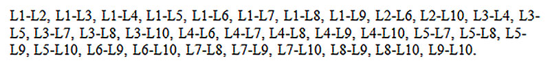
Figure 2. Blind/buried vias by connected layers.
Impedance control. The designers referenced the signals on the top and bottom layer to the adjacent ground plane. Likewise, signals on other layers are similarly referenced to ground planes adjacent to them. High-speed signal routing on an innerlayer is sandwiched between ground and power planes. Careful design of trace width, spacing and prepreg thickness has led to a tight control over single-ended and differential impedance, as shown by calculations in FIGURE 3.
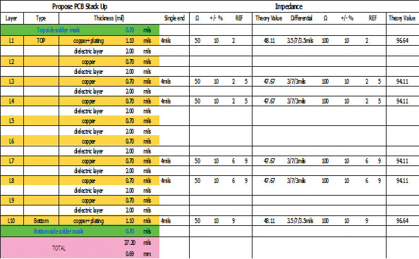
Figure 3. Impedance calculations.
is chief executive officer of Rush PCB, a printed circuit design, fabrication and assembly company (rushpcb.com); roy@rushpcb.com.


Press Releases
- Javad EMS Upgrades Through-Hole Soldering Capacity with New SEHO PowerWave System
- Sharpen Your Selective Soldering Skills with Kurtz Ersa's July VERSAFLOW 4/55 Training
- Omron Advances Inspection Technology with NVIDIA Omniverse and Metropolis
- Seika Machinery’s SMI 2026 Webinar Series Continues with Focus on PCB Cleaning Before Solder Paste Printing