

Understanding and Eliminating Mid-Chip Solder Balls
 One approach: Aperture designs that reduce paste volume from the inside wall.
While the primary theme of this column over the past few years has been miniaturization’s impact on stencil printing, standard SMT process challenges are alive and well. In many applications, where average device dimensions are large compared to the latest package footprints, reducing traditional defects is still a battle. One such frustration: mid-chip solder balls. To understand how to correct this well-known defect, one must appreciate the origin.
Mid-chip solder balls are most often observed with passive devices, specifically, resistors and capacitors. Since these chips have terminations on each end, solder paste material is deposited on two corresponding pads on the board; an open space of solder mask-defined PCB lies between them.
In most cases, once the passive component is placed, everything appears fine. The problems generally arise during reflow. Each termination forms a solder joint, defined by the pad size, the size of the termination and the volume of solder paste on the pad. If all things are equal, reflowing the material results in a beautiful meniscus of a joint that rises halfway up the terminated sides, and that’s it. When all the elements aren’t in balance, and too much solder paste is present, however, there is nowhere for excess reflowed material to go except underneath the device. Molten solder is designed to move. so, if it doesn’t become part of the joint, it goes underneath the component and, in most cases, finds its way out in the form of a solder ball (FIGURE 1). Generally, the mid-chip solder ball sits at the edge of the device, only adhered by flux residue. If it becomes dislodged, the satellite solder ball can be detrimental, potentially intersecting other terminations and causing an intermittent failure in the form of a short. Depending on the resistor or capacitor standoff, there are cases where the rogue solder can remain trapped underneath the component and not escape out the side. The majority, however, are seen outside of the device.
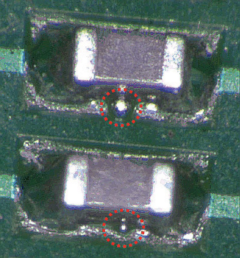
Figure 1. An 0402 device with mid-chip ball defect.
My observation among our wide spectrum of customers is mid-chip solder balling tends to occur more with larger components because they require a larger volume of paste to create the solder joint. As miniaturization has taken hold, mid-chip solder balling on passives from about 0201s and below seems less frequent than on larger 0805s, 0603s and 0402s. In fact, use of these larger components has remained pretty steady, making the mid-chip solder ball one of the most often observed defects with mainstream SMT passive devices.
Factors such as solder paste formulation and reflow profile optimization can affect formation – and also prevention – of mid-chip solder balls. Most familiar with this phenomenon, however, would agree that one of the most impactful approaches to minimization of mid-chip solder balling is through modified stencil aperture design. In general, the aim is to reduce the amount of solder paste on the pad to prevent excess solder from moving underneath the resistor or capacitor during reflow. However, because of multiple factors, just a straight percentage reduction around the entire aperture perimeter isn’t necessarily the best technique.
Ideally, resistor and capacitor manufacturers, board designers and PCB fabricators should follow IPC specs. The reality is this isn’t always the case. I’d bet if you looked at 0402 pad designs for three or four different customers, all of them would be slightly different. Each has their own libraries. One might have the width a little larger for a supplier or customer. Another may round the pads off to a more oblong shape, while one will have the length a bit longer because of accuracy issues. Different pad designs mean dissimilar aperture designs, resulting in varying volume-to-pad ratios for different customers. Plus, although the components are in spec, they may have slight variations in terminations. At the end of the day, this minefield means there are different solder paste requirements, and not one mid-chip solder balling reduction solution will fit all.
In general, what has proven most effective are aperture designs that reduce paste volume from the inside wall of the aperture instead of around the entire perimeter. Our company usually advises to begin with the “home plate” design, which is successful in most cases. For the other 20%, where the home plate aperture doesn’t suffice, modified interior wall reduction designs such as the “crown” or the “U-shape” have delivered (FIGURE 2). As is often the case with SMT, modifications at the front of the line can pay dividends in end-of-line-yield. This is most certainly the situation for the elimination of mid-chip solder balls.
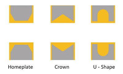
Figure 2. These aperture designs have proven effective in significantly reducing mid-chip solder balling.
is global applied process engineering manager at ASM Assembly Systems, Printing Solutions Division (asmpt.com); clive.ashmore@asmpt.com. His column appears bimonthly.


Press Releases
- Orbit Technologies accelerates growth and doubles production capacity with Europlacer iineo placement machine
- CE3S Brings Back Free ANSI/ESD S20.20 Training Series This August with Desco Industries
- Green Circuits Names Adam Szychowski Chief Revenue Officer
- MicroCare Appoints Doug Kay as Director of Market and New Business Development