

Aligning Six Sigma Tools with Process Reality
Published: 02 March 2023
by Filemon Sagrero
 Identify the areas of variance in stencil design and adjust SPI programming accordingly.
Automated inline solder process inspection (SPI) has the potential to deliver some of the highest value among all inspection steps because defects caught at this point in the process require minimal rework. It is simply a matter of cleaning solder paste off the printed circuit board (PCB). Additionally, good printing performance typically represents 80% of a successful SMT assembly process. As the bulk of workmanship-related defects tend to track back to deficiencies in solder paste deposition, closely monitoring control limits in this area has a substantial impact on eliminating defect opportunities.
Industry 4.0 technology, which connects production equipment and enables automatic correction based on trends data from SPI or automated inspection (AOI) equipment, opens the door to even better process control. As inspection imaging technologies have improved from 2-D to 3-D, the focus on solder paste inspection has gone from paste height to measurements which include volume and area as part of good process control.
Automated inspection equipment is only as good as its programming, however. As a result, variations in stencil design created to address design for manufacturability (DfM) considerations can create issues in the way SPI equipment calculates process capability.
For example, with simple stencil design and good process control, data points measured at SPI following the printing step follow a normal distribution with a single peak, as shown in FIGURE 1.
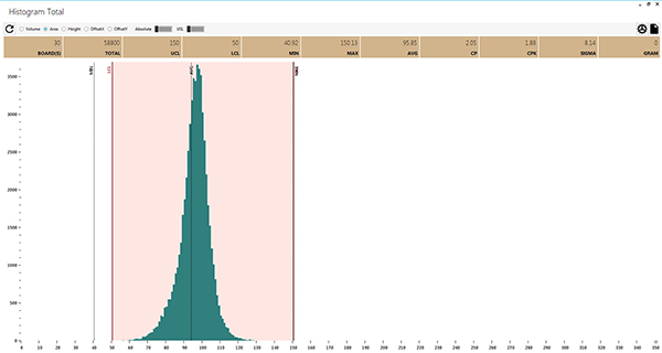
Figure 1. Typical normal distribution.
In some cases, the data points may form two peaks, as shown in FIGURE 2. This is known as a bimodal distribution. Each of the peaks represents a separate group data.
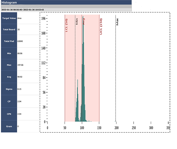
Figure 2. Bimodal distribution.
Typically, the root cause of this datapoint distribution is related to stencil design. In densely populated printed circuit board assemblies (PCBAs) or those with variations in component profiles, the PCB designer may modify the stencil design to add special geometries or steps that increase or reduce solder paste thickness to compensate for components with low or high profiles that require extra or less solder paste volume. To compensate for this, the manufacturing engineering team needs to review the stencil design for these variations and then debug the SPI equipment’s programming to indicate the areas with different solder thickness. Specification limits in accordance with IPC-7725, “Requirements for Solder Paste Printing,” should be set for each subgroup of components.
For example, a stencil was designed with 4 mil apertures with a step up to 6 mils for a few components. Prior to any programming adjustments, the Cpk was 0.67. The programming was adjusted to track data for two subgroups of components based on aperture size. This eliminated the errors caused by mixing data and enabled Cpk to be tracked for each subgroup. The result was a Cpk by subgroup of 1.92, demonstrating the process was aligned with specifications.
This illustrates the importance of identifying areas of variance in stencil design and adjusting SPI programming as part of the new product introduction (NPI) process. Automated inspection technologies offer significant advantages in process control. As this example illustrates, machine programming needs to account for variances built into stencil design to adequately utilize Six Sigma core tools to measure process performance.
is continuous improvement engineer at SigmaTron International (sigmatronintl.com) and a Six Sigma Black Belt; filemon.sagrero@sigmatronintl.com.


