

Solder Fillet Lifting or Pad Lift

Is a change to the acceptability standard needed?
Solder fillet/pad lifting has been found in selective, wave and intrusive reflow soldering. It has not, to date, been seen to cause a reliability problem, and is not always associated with all through-hole joints on a single board.
A solder joint can be perfectly formed, yet either the edge of the pad is lifted from the surface of the laminate, or the solder fillet tip lifts from the edge of the soldered pad. Both conditions are highlighted in IPC-A-610F, Acceptability of Electronic Assemblies for lead-free materials only. It is considered acceptable for Class 1, 2 and 3 products.
FIGURE 1 shows pad lifting from the surface of the laminate. This type of issue was experienced in the past with SnPb when soldering thick multilayer boards, where the expansion and contraction of the board after soldering lifted the copper pad from the substrate.
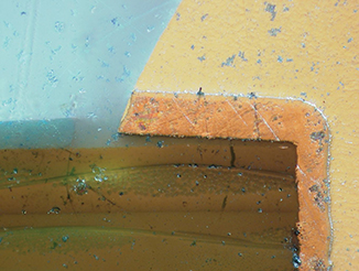
Figure 1. Pad lifting from surface of laminate.
The same phenomenon has been seen on some samples from these projects. FIGURE 2 shows the solder fillet lifting from the surface of the copper pad. This can be seen on SnCu and SAC alloys, which would be acceptable under IPC standards. However, where it happens on high melting point (HMP) solder, which is Pb-based, it would not be acceptable, suggesting a need to change the statements in IPC-A-610 that relate only to Pb-free exceptions.
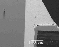
Figure 2. Solder fillet lifting from surface of copper pad.
These are typical defects shown in the National Physical Laboratory’s interactive assembly and soldering defects database. The database (http://defectsdatabase.npl.co.uk), available to all this publication’s readers, allows engineers to search and view countless defects and solutions, or to submit defects online. To complement the defect of the month, NPL features the Defect Video of the Month, presented online by Bob Willis. This describes over 20 different failure modes, many with video examples of the defect occurring in real time.
is with the National Physical Laboratory Industry and Innovation division (npl.co.uk); chris.hunt@npl.co.uk. His column appears monthly.
Register now for PCB West, the Silicon Valley's largest trade show for the printed circuit industry, taking place Sept. 13-15 in Santa Clara: PCBWEST.COM


Press Releases
- Javad EMS Upgrades Through-Hole Soldering Capacity with New SEHO PowerWave System
- Sharpen Your Selective Soldering Skills with Kurtz Ersa's July VERSAFLOW 4/55 Training
- Omron Advances Inspection Technology with NVIDIA Omniverse and Metropolis
- Seika Machinery’s SMI 2026 Webinar Series Continues with Focus on PCB Cleaning Before Solder Paste Printing