

2005 Articles
How Offline Programming Speeds NPI
New tools debug and verify at placement, before releasing product to the floor.
NPI anyone? Don’t answer too quickly. NPI, or new product introduction, is a necessary evil. For an OEM it is an opportunity to release new products. For a contract manufacturer, it means good revenue. But for the lowly process engineer who takes it head-on, NPI can be a living nightmare. Those long days addressing process, material and machine issues are just the tip of the iceberg. Some familiar scenerios: At an OEM is the product development engineer who likes to hang around during a build with a smile – probably the only one smiling – while the complex design is in the works; at an EMS firm are endless voicemails from the customer, indecision and management ensuring an on-time delivery.
Other than badgering NPI, this article discusses building that small number of PCBs as quickly and efficiently as possible. Some powerful solutions are available to address NPI and double machine utilization.
NPI is the assembly of a unique product for the first time on the production line. This typically involves production of a small number of PCBs, usually 25 to 50, with cutting-edge technology. The goal of NPI – other than driving process engineers insane – is to turn incoming data and materials into finished product as quickly and efficiently as possible with minimal scrap and rework.
Typical NPI production lines are low-volume, high-mix and must be able to run most new technologies. The machine that dictates much of the line capability is the placement equipment. Pick-and-place equipment should permit at least 150 to 200 unique component types and should be able to accommodate components in tubes, trays and on tape. They are usually standalone work cells with input and output buffering but are occasionally in-line (with a reflow oven).
In our experience, machine selection for this application is driven more by price than by technology. Lower-cost placement equipment is typically selected because of the difficulty of justifying higher capital for low-volume production. This selection process results in machines that are slower and incompatible with higher production lines. These machines require excess time for non-production activities such as programming and setup. Such placement machines also provide less accuracy, resulting in more rework and higher component use. These factors result in low machine efficiency and utilization.
The metric for a successful NPI operation is how many boards can be produced in a specified period of time with the highest yield and lowest component waste. The drivers for success are flexible equipment, ease-of-programming with offline capability, offline feeder setup, quick first-article test capability and maximum machine utilization. Today’s typical NPI process is iterative, requiring a first-article run, typically on a double-sided “sticky tape” board, error discovery and program debugging at the machines. This iterative process results in high component waste and machine downtime. A better method would be offline programming, setup and verification, coupled with offline debugging to increase machine utilization and eliminate scrap.
Placement equipment is usually programmed with ASCII or CAD data offline. The next step is to generate setup sheets and setup feeders offline. Novel software enables programmers to superimpose or overlay board Gerber data (silkscreen and solder paste layers) over a programmed board to debug for placement angles or polarities by comparing with the silkscreen layer. Checks can also be run on the component shape definition and centroid location by making comparisons to the solder paste layer. This program verification and debugging is performed offline, requiring no machine time or board production (thus eliminating scrap). Figure 1 shows a screenshot of a programmed board with a superimposed assembly drawing (silkscreen and solder paste layers merged as one).
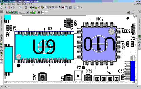 FIGURE 1: Screenshot of silkscreen and solder paste layer superimposed on a placement list.
 |
In the figure, location U10 has the correct centroid and component shape with an incorrect placement angle. Location U9 has an SSOP66 assigned to it, but after further comparison with the solder paste layer, we realize the pitch value of the assigned component shape is incorrect. These checks could be performed only after the assembly kit was released to the manufacturing floor or on the machine, costing precious production time.
Software adds capabilities for process inspection. Figure 2 shows a normal view of a BGA package on a board. Figure 3 shows a simulated close-up x-ray view of the BGA, permitting the programmer to inspect the component for the correct centroid location, placement angle and ball and pitch definition. This is a powerful feature to check flip chips, µBGAs and other packages that have lead/ball definitions hidden under component body.
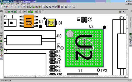 FIGURE 2: BGA in a normal view.
 |
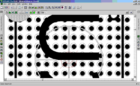 FIGURE 3: Closeup x-ray view of the BGA package.
 |
Board programming and component definition are only half the solution to the NPI puzzle. The other half is proper offline setup. Here, the software tool generates graphic-rich setup sheets for offline setup. Figure 4 is a screenshot of a typical setup sheet with feeder size, location and component shown, the latter including the polarity mark to verify the pick-up angle. An operator can verify that the component has the correct definition, feeder size and pickup angle, and highlight any errors offline while another job is being built on the machine. These tools enable 98% of debugging to be conducted offline, before the job is released to the floor.
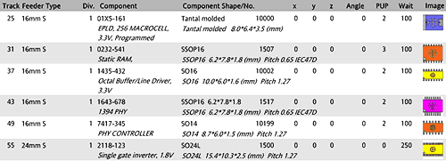 FIGURE 4: A software setup sheet.
 |
For high machine utilization, equipment needs to be in a production mode – building boards – and not used for debugging programs. The ability to superimpose Gerber data, assembly drawings and scanned images of boards (as a bitmap file) on the programmed board helps verify component definition, placement angles and centroid data. X-ray type capability in the software further enhances the process by checking BGAs, connectors, µBGAs, chip-scale packages and other components for proper placement and orientation. Finally, graphic-rich setup sheets help perform a sanity check on pick-up angle and component definition. Process engineers can then watch for potential pitfalls ahead of time.
Sunil Chhabra is senior applications engineer and Mark Ogden is product manager at Siemens Logistics and Assembly (siemens.com); sunil.chhabra@siemens.com.


Press Releases
- The SearchWorks Group Shares Mid-Year Read on the EMS Talent Market
- Altus Announces Return of ‘Factory of the Future’ for 2026
- Circuit Technology Center, Inc. Expands High-Volume BGA Reballing Capacity with Investment in Additional Reflow Oven
- SEMI And Global Net Corp. Release New Report On Glass Core Substrate Market And Development Trends For Semiconductors