

2005 Articles
The Relationship of Components, Alloys and Fluxes, Part 1
Call it a love triangle – or a Bermuda Triangle. Either way, the best alloy may be determined by the end-application.

Lead has been an indispensable element in solders due to its high ductility, reasonable mechanical strength, low eutectic melting temperature with tin, low surface tension and low cost. Lead-free soldering requirements are an earthquake to the lead infrastructure that has been evolving for several decades. Within the past few years, the relationship among components, alloys and fluxes has already reshuffled. Although the dust has not settled, a picture of this new relationship is emerging. Changes in alloys not only directly impact components and fluxes, but also the relationship between components and fluxes, which in turn impacts the alloys.
Alloys vs. Components
High temperature stability. Perhaps the biggest impact on components is the requirement of higher thermal stability. With mainstream solder for SMT changing from eutectic SnPb to higher melting temperature systems such as eutectic SnAgCu (217°C), eutectic SnAg (221°C) or eutectic SnCu (227°C), the soldering temperature inevitably has to be raised, with a consequent increase for component thermal stability. As reflected in IPC/JEDEC J-STD-020C, with an increase in melting temperature to 217°C from 183°C, the thermal stability requirement rises about 20°C. On the other hand, moisture sensitivity would drop one to three levels with 260°C reflow peak temperature, and new molding compounds would be desired to improve the performance – at additional packaging cost.1
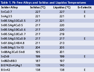
The interaction between solder alloy and components is two-way. The impact of a high solder melting temperature is very harsh, particularly for large boards in applications such as servers or telecommunication systems in which the temperature gradient across the board can be greater than 40°C and the maximum temperature experienced by some components can be over 270°C. In other words, the thermal stability of components has to be upgraded to that temperature, unless the melting temperature of solder alloys is reduced. The latter appears to be an easier solution, and has been adopted by industry. Table 1 shows melting temperatures of some viable Pb-free solders, including some low melting alloys. A 10° to 20°C decrease in melting temperature is sufficient to permit components to survive in large-board situations. Alloys such as Sn86.9Ag3.1In10, Sn88Ag3Cu0.5In8 or Sn89Zn8Bi3 are considered viable for this purpose. Bi57Sn42Ag1 and Bi58Sn are also possible options. The latter has been used by IBM for wave soldering for three decades. However, the melting temperature of eutectic BiSn or near-eutectic BiSnAg1 may be so low that their service temperature range is compromised.
1. Internal Solder Alloys
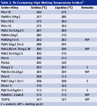
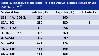
High melting solders. Due to the process hierarchy consideration, the internal solder joints of a package often need to be high in melting temperature so that the subsequent board-level assembly will not cause remelt of those internal joints. Remelt of internal solder joints may cause die drifting, solder extrusion and damage on wire bonding. With SAC alloys having a melting temperature around 217°C being adopted as a mainstream solder for SMT assembly, and with components possibly reaching 260°C upon reflow, internal solder joints should have a solidus temperature above 260°C, preferably above 280°C. Table 2 shows some Pb-containing solders with solidus no less than 260°C.2 By considering alloys with melting temperatures as high as 500°C, still very few Pb-free alloys meet this relaxed requirement, as shown in Table 3, and none are acceptable as a drop-in Pb-free replacement for high-temperature, Pb-containing solders.2 Gaps in performance include melting temperature and range, solder wetting, solder ductility, mechanical strength, thermal fatigue, electromigration and cost. Due to these unresolved gaps, lead is exempted in certain RoHS applications: 1) solder joints with lead content greater than 85%, 2) pin-to-package connection with 80 to 85% lead and 3) lead used in flip-chip solder joints within packages.
Medium melting solders. For internal solder joint applications where remelting is not a concern, solder mechanical or thermal fatigue behavior becomes the focus. Frear et al. reported in 2001 that eutectic SnCu performed best in flip-chip applications.3 Clech in 2004 analyzed some published data (Figure 1) expressing the correlations of characteristic life to cyclic shear strain range for bare chip assemblies for SnCu, SnPb and SAC assemblies by trendlines.4 The analysis indicates that, under high cyclic shear strain range, eutectic SnCu with a higher ductility exhibits a longer characteristic life. The results suggest that, in low-strain applications, a more ductile solder experiences an earlier loss of structural integrity and therefore earlier failure. In high-strain applications, this faster creep deformation results in a shorter life than in low-strain applications. However, this deformation also avoids early cracking caused by excessively large strains, and therefore outlives solders with low ductility. On the other hand, more brittle solders such as SnAgCu or SnAg could not relieve the stress caused by large strains, and consequently suffer early cracking at weak spots of the system. In other words, the best alloy choice is determined by the end-application.
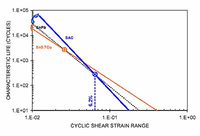 FIGURE 1: Correlations of characteristic life to cyclic shear strain range for bare chip assemblies: power-law trendlines for SnCu, SnPb and SAC assemblies.4
 |
Alpha particle emission. An alpha particle is a nuclear particle that contains two protons and two neutrons. The alpha particle strips electrons from atoms such as 28Si as it passes through the electron cloud of an adjacent atom, thus producing charge along their path, leaving a trail of electrons and holes. When enough electrons were knocked out of an IC and accumulated in a capacitor, it switched the capacitor from 0 to 1 or from 1 to 0 and resulted in a so-called “soft error.” The distance an alpha particle travels through the semiconductor package ranges from 7 µm for Au to 24 µm for Si and 28 µm for polyimide. For high I/O devices, solder bumps have to be placed everywhere on the IC surface, hence a low alpha emission solder will be required.5
Within common solder constituents, lead has been identified as the primary source of alpha particles. Both 214Pb and 210Pb contribute to alpha emission, with 210Pb being the primary source due to its considerably longer half life (Figure 2). Most of the elements involved in viable Pb-free alternatives, either as major constituents or as possible minor additives such as tin, indium, silver, copper, antimony, zinc, germanium, nickel and gold, have no isotopes which will release alpha particles; all considered safe. Bismuth may have an issue due to the existence of radioactive 214Bi, which will convert into stable 206Pb in about 24 years. 212Bi would also undergo alpha decay and cause concerns for soft error.5
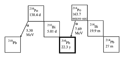 FIGURE 2: Secular equilibrium of lead.
 |
Other than Bi-containing alloys, low alpha emission can be achieved by controlling lead impurity levels. The alpha emission rate of typical pure lead is about 10-102 count/cm2/hr. Solders currently in use have alpha emission levels from 0.05 to 0.01 count/cm2/hr. (LC2 level). To reduce alpha emission rate from 102 to 10-2 count/cm2/hr., the lead content in Pb-free solders will have to be lowered by four orders of magnitude, or to 100 ppm or below. This is easily achievable, since tin is the primary source of lead contamination, and lead impurity in tin metal often ranges from 50 to 200 ppm. In other words, the requirement on maximum lead impurity permitted can be met by screening tin lots for lead content with a reasonably high pass rate. However, the same cannot be said for future requirements in which the alpha emission rate may need to be as low as 10-3 count/cm2/hr. (LC3 level).5
2. BGA Solder Balls
Fragility. Similar to SMT assembly applications, SAC has also been adopted for BGA solder balls. The alloys employed include SAC305, SAC387, SAC396 and SAC405. However, unlike other SMT components, the fragility of BGA SAC solder joints appears to be considerably poorer than that of BGA SnPb joints for both NiAu and OSP surface finishes, particularly in the former case. This difference manifests especially in the drop test. BGA SAC joint fragility has been attributed to inconsistent plating quality of the copper pad,6 Kirkendall void formation,7 low solder ductility and intermetallics.8
To resolve the issues, approaches have been taken to develop alloys with better resistance against fragility. The most popular approach is increasing the solder ductility by decreasing the Ag and Cu content; reducing Ag is the most effective means. While Ag down to 1.5 or 1% has been considered favorable, Date et. al. further claim the desired Ag content is 0 to 1%, with Cu at 0.5 to 0.7%. With NiAu BGA surface finish, those alloys outperformed SnPb in drop tests.8
Adding small amounts of other elements is an attractive way to suppress intermetallic formation. Elements such as Ge, Ni and Zn have showed promising results. Zn has also reduced Kirkendall void formation by suppressing Cu3Sn formation on copper pads. Maintaining some Cu in Pb-free solders is also considered helpful in curtailing intermetallic formation on NiAu.8 The effect of adding additional elements varies depending on the type of finish involved.
Intermetallic plates. Ag in Pb-free solders contributes to fragility of joints and to the formation of large intermetallic plates. Figure 3 shows AgSn intermetallic plates formed in the solder joint of SAC on Cu after being reflowed twice at 260°C and heavy etching.9 The plates may grow across the entire solder joint, and may protrude out of the joint itself. The probability of AgSn plate formation is aggravated with slow cooling and thermal aging, and decreases with decreasing content of Ag. An IBM study indicated that the probability of large AgSn plates observed in solder balls with SAC alloys solidified at a rate of 0.02°C/sec. is 76/100 for SAC387, 9/200 for SAC309, 1/200 for SAC259 and 0/200 for SAC209. IBM noted that Sn97Ag2.3Cu0.5Bi0.2 is desirable for ball composition, with Bi added to prevent tin pest formation.10
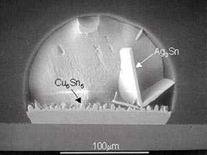 FIGURE 3: Intermetallic compounds formed in the solder joint of Sn95.5Ag3.8Cu0.7 on Cu.9
 |
3. Small Forms
With continuous miniaturization of electronics, discretes such as chip capacitors or resistors are also shifting toward 0402, 0201 or 01005. An immediate impact is the rapid increase in tombstoning rates. Although this problem can be countered by optimizing fluxes, designs or profiles,11 the most effective approach is solder alloy optimization. Figure 4 shows results of an Indium study on tombstoning rates of solder pastes. Tombstoning of SAC is affected by solder composition, and is dictated by the wetting at the onset of the paste melting stage. A maximal tombstoning rate is observed at the ternary eutectic composition Sn95.5Ag3.5Cu1. The tombstoning rate decreases with increasing deviation in Ag content from this composition. A DSC study indicates this is mainly due to the increasing presence of pasty phase in the solders, which results in a slower wetting speed at the onset of solder paste melting. Surface tension plays a minor role, as lower surface tension correlates with a higher tombstoning rate. SAC composition with an Ag content lower than 3.5%, such as Ag2.5, is more favorable to reduce tombstoning.12
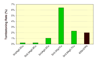 FIGURE 4: Tombstoning rate of solder pastes under vapor phase reflow. SAC and SnPb pastes were reflowed at 260° and 215°C, respectively.
 |
4. Component Finishes
Pb-free surface finishes of components include Sn, SnBi, SnCu, SnAg, NiAu and NiPdAu. Among those, Sn is favored for passives, SnBi is common for leadframes and NiPdAu is popular for pre-plated leadframes.
ýn is solderable and cheap. Concerns over tin whiskers (caused by compressive stress in the tin layer) must be addressed. Under isothermal conditions, the compressive stress generation is dominated by IMC formation at grain boundaries whereas under temperature cycling conditions, stress generation is dominated by CTE mismatch between Sn and the metalization underneath. Measures shown relatively effective in curtailing tin whiskers include Ni-barrier plating, thin Sn layer, baking treatment and alloying with Bi.
NiPdAu is both wire bondable and solderable, and can be used on pre-plated leadframes without the need for selective plating. This simplified process results in a lower manufacturing cost than that of Sn plating when used on pre-plated leadframes. A tradeoff may be reduced joint strength due to reduced wetting.13
5. Components Assembled with Mixed Alloys
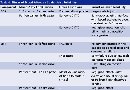
Whether a forward or backward compatibility situation, mixed alloys are inevitable during the transition. In general, Pb contamination often significantly compromises reliability, and should be avoided when possible. Table 4 lists mixed alloys at component assembly and their impact on solder joint reliability.
References
- Lead-Free Component Team, “Component Implications of Lead-Free Reflow Assembly,” IPC/NEMI Symposium on Lead-Free Electronics, September 2002.
- Indium Corp. of America data sheet.
- D.R. Frear, J.W. Jang, J.K. Lin and C. Zhang, "Pb-Free Solders for Flip Chip Interconnects,” JOM, June 2001, pp. 28-38.
- J-P. Clech, “Lead-Free and Mixed Assembly Solder Joint Reliability Trends,” IPC Apex, February 2004.
- N-C. Lee, “Lead-Free Soldering and Low Alpha Solders for Wafer Level Interconnects,” SMTA International, September 2000.
- C. Chiu, K. Zeng, R. Stierman, D. Edwards and K. Ano, “Effect of Thermal Aging on Board Level Drop Reliability for Pb-free BGA Packages,” ECTC, June 2004, p. 1256.
- D. Henderson, “On the question of SAC solder alloy – Cu pad solder joint fragility,” Webcast on SAC Solder Joint Fragility, September 2004.
- M. Date, T. Shoji, M. Fujiyoshi and K. Sato, "Pb-free Solder Ball with Higher Impact Reliability," Intel Pb-free Technology Forum, July 2005.
- T. Y. Lee, W. J. Choi, K. N. Tu, J. W. Jang, S. M. Kuo, J. K. Lin, D. R. Frear, K. Zeng and J. K. Kivilahti, "Morphology, Kinetics, and Thermodynamics of Solid State Aging of Eutectic SnPb and Pb-Free Solders (Sn3.5Ag, Sn3.8Ag0.7Cu, and Sn0.7Cu) on Cu,” J. Mater. Res. 17 (2), 2002.
- S. K. Kang, W. K. Choi, D-Y. Shih, D. W. Henderson, T. Gosselin, A. Sarkhel, C. Goldsmith and K. J. Puttlitz, “Formation of Ag3Sn Plates in Sn-Ag-Cu Alloys and Optimization of their Alloy Composition,” Electronic Components & Technology Conference, May 2003.
- N-C. Lee, “Reflow soldering processing and troubleshooting SMT, BGA, CSP and Flip Chip Technologies,” Newnes, 2001, p. 288.
- B. Huang and N-C. Lee, “Conquer Tombstoning in Lead-Free Soldering,” IPC Apex, February 2004.
- C. Jensen, F. Kuhlman and M. Pepples, “Robust Optimization of a Lead Free SMT Process,” IPC Apex, March 2003.
Ed.: Part 2, a look at the relationship between alloys and fluxes and components and fluxes, will be published in December.
Dr. Ning-Cheng Lee is vice president of technology at Indium Corp. of America (indium.com); nclee@indium.com.


Press Releases
- Javad EMS Upgrades Through-Hole Soldering Capacity with New SEHO PowerWave System
- Sharpen Your Selective Soldering Skills with Kurtz Ersa's July VERSAFLOW 4/55 Training
- Omron Advances Inspection Technology with NVIDIA Omniverse and Metropolis
- Seika Machinery’s SMI 2026 Webinar Series Continues with Focus on PCB Cleaning Before Solder Paste Printing