

2005 Articles
Spray Fluxing for Pb-Free Wave Soldering
Refined spray application and deposits are musts for next-generation processes.
Spray fluxing applications are not immune from problems during Pb-free solder processing. In fact, good flux chemistry and flux deposition control are critical to successful Pb-free wave soldering.
During spray applications, liquids are atomized to produce a fine mist composed of liquid droplets. To form a fine mist fluxes need to have low viscosity and low surface tension. Viscosity and surface tension of a flux depends on the solids content and type of the solvent system used in the product formulation.
Based on the solids content, wave soldering fluxes fall into three major categories:
- Low solids (<5%).
- Medium solids (<10%).
- High solids (>10%).
Low solids, alcohol-based fluxes are easy to spray because of the low surface tension of alcohol and low viscosity. Medium and high solids content fluxes, no-clean or water soluble, water- or alcohol-based, cannot be used in spray applications unless they are formulated with proper solvent systems and additives to produce a fine mist for good penetration and proper wetting of the surfaces to be joined.
Flux needs to come into intimate contact with molten solder and the surfaces to be joined so that it can:
- Decrease the dihedral angle (the angle between the liquid solder and the surfaces to be joined), thus enabling the solder to wet the pad and component surfaces better;
- Completely wet the surfaces to be joined (metal, OSP, etc.) and wick up through-holes, removing oxides formed on the surface, thus making the surface available for total contact with the solder;
- Penetrate the OSP and provide a barrier on the cleaned metallic surface; otherwise the freshly exposed surfaces will easily reoxidize in the atmosphere, accelerated by the elevated soldering temperatures.
When solder is introduced on the fluxed surfaces to be joined, the solder will then displace the flux and bond with the base metal, thus promoting 100% wetting.
However, without good flux deposition even the best flux chemistry cannot do its job. Flux deposition is the process of applying liquid flux uniformly on all the 3-D surfaces of a board assembly that will be exposed to molten solder.
In the ideal no-clean soldering process, flux applied to the board is consumed in the soldering process, virtually eliminating post-soldering flux residue. If too much flux is applied, excess post-soldering flux residue will result. It is critical to apply the minimum amount of flux required to facilitate soldering. To do so, a spray fluxing system must apply the flux uniformly to the bottom surface of the board and into the through-holes. To maintain this process throughout a production shift, the spray fluxing system must have the capability of repeating the preset flux deposition amount with little variation.
Flux manufacturers provide guidelines for typical flux deposition range for a chosen flux. Flux deposition is specified in micrograms of flux solids per square inch (or square centimeter). A typical deposition range might be from 750 to 2,500 µg/in2 of flux solids on the board.
The best no-clean processes use the smallest possible amount of flux solids while still achieving acceptable soldering results.
Flux Application Experiments
Three experiments were recently conducted to measure the performance of a fluxing system. (The measurements can also be used to create an operating process matrix to assist in future setups.) The parameters measured were:
- Flux flow rates to the fluxer spray head.
- Flux weight deposited per PCB.
- Flux deposition uniformity and through-hole penetration.
Experiment 1: Flux Flow Rates
Objective: The spray fluxing system used for this test delivers flux to the spray head via a positive displacement gear pump and ON/OFF solenoid valve. The basis for this test was to measure the volume of flux flow to the fluxer spray head based on a percentage of pump speed (30 to 100%), and to measure for repeatability. Low solids, no-clean, VOC-free (water-based) flux was used for this test.
Test: Measurements of 30 to 100% pump speed were taken, six times each, for 60 sec. The flux was collected and the volume was measured with a graduated cylinder. Results are in Table 1 and plotted in Figure 1. The deviation of the measurements is less than one cc. Flux flow rate depends linearly on percent pump speed with excellent correlation (>0.99999). The conclusion: Flux flow rate to the spray head is highly repeatable and increases linearly relative to pump speed.
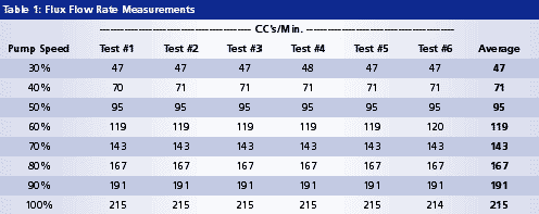
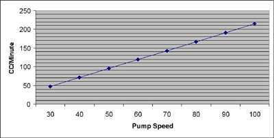 FIGURE 1: Flux flow rate chart.
 |
Experiment 2: Flux Weight per PCB
Objective: The amount of flux the spray fluxing system deposits on a PCB depends on three variables:
- Flux flow rate to the spray head.
- Traversing speed of the spray head.
- Spray pattern pitch (overlap of the spray strokes).
If flux flow rate, spray head traversing speed or spray pattern pitch are changed, total flux weight applied to a PCB will change. The purpose of this test was to measure how traversing speed affects the amount of flux applied to a PCB (while flux flow rate and spray pattern pitch remained constant), and to prove good repeatability.
Test: Experiments were conducted with the following inputs:
- Forty percent flux pump speed at a traversing speed of 10" per sec.
- Forty percent flux pump speed at a traversing speed of 15" per sec.
The spray fluxing system was programmed to target a spray area of 63 in2. When the system was activated, flux flow was diverted to a graduated beaker for measurement.
As shown in Table 2, the traversing speed directly affects the amount of flux applied to the PCB. The precise control over traversing speed and flux flow rate provides a flux deposition variation better than ±1%.
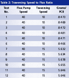
Once machine parameters have been established for a particular PCB recipe, flux deposition can be calculated using a parametric analysis tool such as a flux deposition calculator (Figure 2).
 FIGURE 2: Flux deposition calculator.
 |
Experiment 3: Flux Deposition Uniformity and Through-Hole Penetration
Objective: The purpose of this test was to measure flux uniformity and through-hole penetration by spraying flux through a test PCB (13" x 8.5" x 0.062" with 0.035" diameter holes on 0.100" centers) onto pH paper. The pattern produced on the pH paper indicates flux through-hole penetration and uniformity. The spray fluxing system produced a flat, rectilinear spray pattern, and passed under each through-hole location twice.
Test: Four trial runs were conducted using the following parameters:
- Spray head pitch (overlap) 2.5"; flux pump speed 30%; spray head traverse speed 15.0 ips.
- Spray head pitch 3.5"; flux pump speed 30%; spray head traverse speed 15.0 ips.
- Spray head pitch 2.5"; flux pump speed 40%; spray head traverse speed 15.0 ips.
- Spray head pitch 3.5"; flux pump speed 40%; spray head traverse speed 15.0 ips.
Conclusion: The resulting pattern on the litmus paper (Figure 3) indicates that flux uniformly penetrated every through-hole with a spray head pitch of 2.5" and flux pump speeds of 30% and 40%.
 FIGURE 3: Representative litmus paper pattern (pitch 2.5", pump 30%, traverse speed 15.0 ips).
 |
A flux developed specifically for spray application and an efficient spray fluxer that deposits flux where it is needed is required to obtain excellent joints during Pb-free wave soldering with spray fluxing. The flux should produce a fine mist when atomized as well as removing oxides from surfaces to be soldered, decreasing the dihedral angle for solder wetting. Spray fluxing systems need to be able to apply the flux repeatedly, uniformly and completely over all surfaces exposed to molten solder. Flux deposition depends on flux flow rate, traverse speed and pitch, and these parameters should be optimized to apply the minimum flux required for good solder joints in wave soldering processes.
Sanju Arora is manager of chemical R&D at the Central Research Center of Cookson Electronics Assembly Materials Group (cookson.com); sarora@cooksonelectronics.com. Stanley Soderstrom is product engineer at Ultrasonic Systems Inc. (ultraspray.com); sjsoderstrom@ultraspray.com.


Press Releases
- The SearchWorks Group Shares Mid-Year Read on the EMS Talent Market
- Altus Announces Return of ‘Factory of the Future’ for 2026
- Circuit Technology Center, Inc. Expands High-Volume BGA Reballing Capacity with Investment in Additional Reflow Oven
- SEMI And Global Net Corp. Release New Report On Glass Core Substrate Market And Development Trends For Semiconductors