

Viewing Solder Joint Cracks in X-Ray

It’s cheaper and faster to inspect by machine over microsection.
Most of my columns have attempted to discuss the “typical,” and often more obvious, solder joint failures that can be seen using x-ray inspection. This is usually the main and most important function of this type of analysis.
Nondestructive inspection of cracks within solder joints or components is also desirous, however, but this is much more difficult to evaluate optically or by x-ray. Even for those joints that are not optically hidden, optical inspection for cracks is likely limited to the very end of the termination and requires a mostly edge-on view at a reasonable magnification (FIGURE 1) to have the best chance of seeing a crack failure. When inspecting fully populated boards, achieving this level of magnification and orientation may be difficult to do optically, and any cracks present will need to be distinct by showing a separation in the joint. If the two halves of the cracked solder are still touching, then analysis may be almost impossible to make. Furthermore, such a crack will be at the end of the termination and not necessarily extending further back into the joint – for example, into the heel fillet of a QFP, which is more crucial to joint integrity. This may mean a cosmetic issue is seen on one joint, and the actual fault may remain hidden elsewhere.
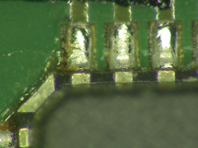 Figure 1. Optical image of QFN joints after 1,000 thermal cycles, where there is an indication of a separation between the joint and pad.
If optical inspection does not help to see cracks, then can x-ray inspection? The first question to ask is, is there sufficient density difference between a cracked and non-cracked joint, so this density difference can be seen as different grayscale levels in the x-ray image? This depends on the board under inspection and the x-ray system capability. The thicker and denser the board, the greater the amount of material the x-rays must pass through before they go through the cracked solder joint. In other words, you have to look for the lower density of the crack against, and over, a much denser background. Second, the better the grayscale sensitivity of the x-ray system, the better the chance to see any subtle differences between cracked and non-cracked joints. This means x-ray inspection can provide an opportunity to see cracks, but it should not necessarily be depended on for quality control because of the potential for low-density variations; additional methods should be included or considered.
Once you have images of suspect joints, my typical rules for x-ray inspection still apply: compare known good and bad examples and look for (in)consistency across all similar joints on the same component/board to confirm the analysis. In the case of cracks, however, also consider that if everything looks consistent, yet electrical tests report otherwise, ask if perhaps the x-ray system is not seeing what you need to.
To illustrate this point and show the subtlety of the grayscale differences likely for cracks, I am grateful to Bob Willis of bobwillis.co.uk (PCB assembly and optical images), Richard Boyle of Henkel (microsection images) and Peter Koch of Yxlon (x-ray images) for the following example. A test board was created and used to investigate thermal cycling failures of QFNs. Joint cracking of QFN packages containing over 40 pins is not uncommon, owing to the planar nature of the device and its positioning on a (likely) pliable surface such as a PCB. The boards were produced with SAC solder paste using a 0.005" stencil. They were reflowed in air in a 10-zone convection oven. The boards were not electrically connected to permit solder joint failures to be detected. X-ray inspection was used after 1,000 and 2,000 cycles, respectively, prior to microsectioning. The boards were visually inspected after approximately 500, 1,000 and 2,000 cycles (Figure 1). After 1,000 cycles, the onset of solder separation on the corner joints of the QFN packages was suspected. At 2,000 cycles it was believed the separation was increasing. FIGURE 2 shows the QFN and the planes across which it was subsequently microsectioned, first along the blue line and then along the red. FIGURE 3 shows a microsection produced from along a section of the blue line and indicates cracks on all joints at that position.
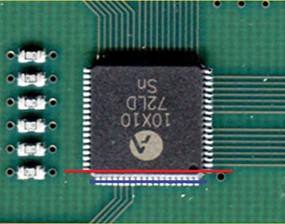 Figure 2. Schematic of the locations of the microsections.
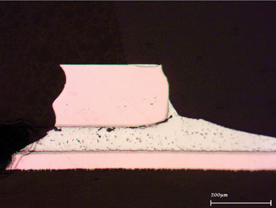 Figure 3. Microsection from along the blue line shown in Figure 2.
FIGURE 4 shows a further microsection from along the red line in Figure 2, where a crack can be seen extending horizontally and under a substantial portion of one of the QFN edge terminations. The first microsection shows only that cracks are present but not how far they extend into the joint.
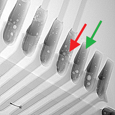 Figure 4. Microsection from along the red line shown in Figure 2. A crack extends across a substantial length of the joint.
Obviously, microsectioning the board is a destructive process, so what can x-ray inspection tell us in this example ahead of cutting the board? FIGURE 5 shows an x-ray image of some of the QFN solder joints. The presence of cracks is shown (and highlighted). This is subtle and needs careful consideration, and comparison against other similar joints, but offers, in this example, some opportunity for seeing cracks nondestructively.
In Figure 5, we see some density variation in the highlighted joint compared to the adjacent joint. These suspicions can be followed up by using other tests and techniques. However, this example is a simple test board; in “real” boards it may be more difficult to see these subtle differences, as they may have many more layers with internal copper traces or other components obscuring the joints from view. Therefore, the use of appropriate oblique angle views to remove obscuring features from the field of view is important.
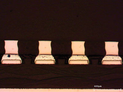 Figure 5. X-ray image of QFN joints prior to microsectioning. The crack seen on the highlighted joint is clearer compared to the adjacent joint.
If you suspect cracks exist, try x-ray inspection before cutting the board. But remember, not all x-ray systems have the same capabilities. To give yourself the best chance, consider the impacts of the board configuration and the sensitivity of the x-ray system. Then carefully analyze the images and compare and (ahem) contrast similar joints.
, is an expert in use and analysis of 2-D and 3-D (CT) x-ray inspection techniques for electronics; dbc@bernard.abel.co.uk.


Press Releases
- Seika Machinery’s SMI 2026 Webinar Series Continues with Focus on PCB Cleaning Before Solder Paste Printing
- Forwessun Expands Testing Capabilities through Strategic TRI Alliance
- Federal Electronics Expands Advanced Manufacturing Capabilities to Support Military and Aerospace Cable Assembly and Wire Harness Programs
- Altus Continues Irish Growth with Expansion of Engineering Team