

Bare Board X-ray Inspection: Start at the Base
 When nondestructive methods are preferred, leverage the x-ray.
The operation and reliability of any electronic assembly is as dependent on the performance, quality and consistency of the bare printed circuit board as it is on quality components and a sound manufacturing process. Without quality bare boards, however excellent the assembly process, whole batches of product will be at risk of failure, as they will have been built on an inherently bad foundation. Add the possibility that the boards may be stored for long periods before being used, perhaps in suboptimal conditions, and we have a recipe for problems within that basic foundation. Bare board quality today is usually so good that many will not expect it to be the cause of an issue until much, much later in the “blame game” of root cause analysis. Assemblers will typically focus first on examining and clearing what they (may) have done, then look at the components. (Remember, everyone at first blames the BGA!) Therefore, appreciating how bare boards are manufactured, understanding their potential areas for failure and having access to appropriate inspection facilities should allow, in principle, those involved in incoming/receiving, or the first step of the assembly process, to identify and minimize bare board issues ahead of release to assembly.
Often, any external bare board problems may be identified simply with optical inspection techniques. If the issue lies within the board, however, it will not be optically visible. For example, consider the possibility of receiving bare boards with poor drilling quality in the vias, perhaps caused by use of a blunt drill bit. One of the potential effects is variation in the plating down the length of the via. Looking inside the board, or at least within small sections of it, to establish if these issues are occurring could be achieved by microsectioning. This is a destructive, time-consuming and expensive process, however, requiring expert interpretation, and analysis is limited to very small sample areas. This makes microsectioning uneconomic to do, especially on a typically low-value component in high-volume manufacture such as the bare board. Further, you are relying on the sample taken to be entirely representative of the whole board and the rest of the batch. Therefore, nondestructive techniques are preferred. This is where x-ray inspection equipment often found within the PCBA manufacturing environment, and usually used for analyzing assembled boards, can also be used to identify bare board issues.
X-ray equipment is used for bare board analysis during manufacture. This is typically for checking alignment and registration of layers. Such checks are coupled with others to maintain and ensure process integrity by the PCB supplier. The x-ray systems commonly used in fabrication processes are adequate for that task. But they tend to have limited technical capabilities and may not be able to identify all the specific issues on finished boards. For example, bare board x-ray systems typically look only from the top down; in other words, they do not offer oblique angle views, and often have a much more limited magnification and resolution in their imaging capability. X-ray systems used for assemblies, in contrast, require all these functionalities to see the smaller, and smallest, features typical of today’s boards. Checking bare boards during manufacture for correct alignment is one thing, but the systems might not permit effective viewing or analysis of other smaller-sized failures or issues that might be present or created during other processing techniques.
Poor drilling quality in the bare board may make it more difficult for copper to cover and maintain equal thickness down the via during plating. This can often be seen nondestructively on a “PCBA-focused” x-ray using an oblique-angle view of the via (FIGURE 1). In this image, the plating thickness variation shows up as nonuniform grayscale along the depth of the via. Using the “PCBA” x-ray for bare boards usually also allows the operator to provide quick and additional analysis over other representative areas on the whole board using the sample manipulation, something that may be more difficult to achieve optically, especially with a manual microscope. FIGURE 2 shows an optical image of the same via. The variation in the plating is also clear, but this type of optical image would not be possible to check a buried via. Ideally, the x-ray image should show a uniform grayscale down the via, indicating smooth, consistent plating (FIGURE 3).
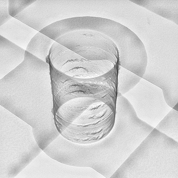
Figure 1. Oblique-angle 2-D x-ray image of via with plating variation down the barrel.
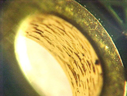
Figure 2. Optical image of via with plating variation down the barrel (courtesy Bob Willis).
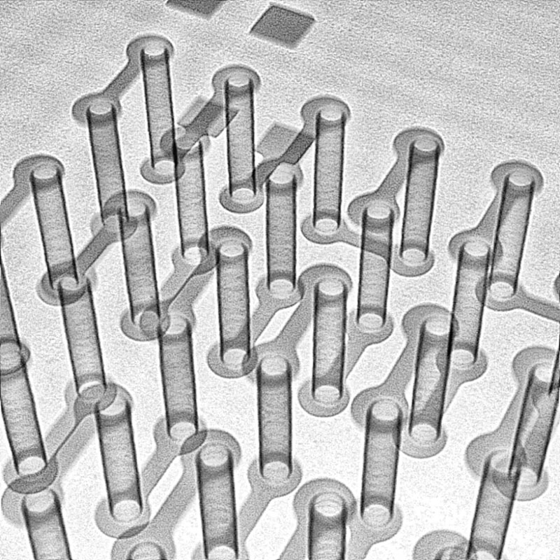
Figure 3. Oblique-angle 2-D x-ray image of vias with consistent plating variation down the barrel.
Once bare boards are received, and/or prior to assembly, consider using PCBA x-ray equipment to inspect and check representative samples and meaningful locations within to see if there are any issues in the bare board. This will require ensuring line personnel and goods received inspectors have the right training and knowledge of the appropriate standards to evaluate bare boards prior to assembly. Such training should include access to, and the encouragement to take, reference optical and x-ray images that highlight what an acceptable board looks like, and an understanding of specific areas of risk within a particular board, which may have been identified through use of microsectioning, such that checking is quicker and more targeted.
So, in addition to the usual tests, consider using available PCBA x-ray equipment on representative bare board samples to validate board quality and give additional confidence the PCBA is based on a firm platform.
Au.: Images courtesy Peter Koch, Yxlon International.
, is an expert in use and analysis of 2-D and 3-D (CT) x-ray inspection techniques for electronics; dbc@bernard.abel.co.uk.


Press Releases
- Javad EMS Upgrades Through-Hole Soldering Capacity with New SEHO PowerWave System
- Sharpen Your Selective Soldering Skills with Kurtz Ersa's July VERSAFLOW 4/55 Training
- Omron Advances Inspection Technology with NVIDIA Omniverse and Metropolis
- Seika Machinery’s SMI 2026 Webinar Series Continues with Focus on PCB Cleaning Before Solder Paste Printing