

A Career in Test Engineering

What the newly minted graduate can expect, and why they should pursue the field.
Technology has never been so exciting, and it will only get more so as we continue to hanker for better ideas and innovation to improve our lives. We are always on the lookout for devices that will feed our insatiable appetite for new gadgets, such as smartphones, mini drones, cameras and other “cool and trendy” items. What many users do not realize are the processes each product has to go through to ensure its usability and functionality for the intended purpose. And behind each of these steps is a test engineer.
The industry is facing a shortage of qualified test engineers. Unfortunately, among the cohorts of new engineering graduates each year, not many choose to build a career as a test engineer, unaware there is actually tremendous growth opportunity for them.
Every product has to undergo multiple steps in every product stage, from prototype and new product introduction to volume production (FIGURE 1).
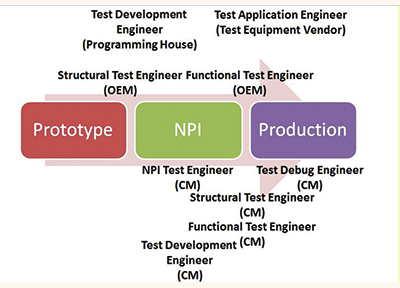
Figure 1. Test engineering roles figure in every stage of electronics production.
So how, exactly, does a fresh graduate become a test engineer? Say you have just graduated with a degree in electronics engineering and are looking for a job. While Googling big electronics companies for an opening, you may stumble on a job opening for test engineer. The job description will sound pretty interesting, with the opportunity to travel and learn new technologies, working closely with other professionals, such as design engineers and managers, and even other test engineers across different time zones. However, there will likely be things you are unfamiliar with, as these topics were probably not specifically covered during your electronics engineering courses. Let’s take a look at some of these topics.
In-circuit test system. ICT is a popular test methodology used in the manufacture of every printed circuit board assembly due to its ability to immediately find manufacturing faults such as open, shorts, wrong value of components and malfunctioning components in the PCBA. ICT has been around since the boom of electronics manufacturing from the early 1980s, and has undergone constant technology refresh to keep abreast with the present technology. The following are some of the tests enabled by ICT systems:
- Shorts and opens. An unpowered test method that tests for unexpected shorts and opens in the PCBA.
- Analog in-circuit. An unpowered test that measures the value of analog devices, such as resistors and capacitors.
- Vectorless Test EP. An unpowered test of the connectivity from each pin on a device to the circuit board. The system uses VTEP hardware to measure the capacitance from a pin of a device to the VTEP probe to determine connectivity.
- Analog functional. A powered test that applies a stimulus to a device or circuit under test and measures its response.
- Mixed testing. A powered test that applies analog functional and digital test methods to a device or circuit.
- Digital in-circuit. A powered test that applies vector patterns to the device and tests for the expected outputs. Digital in-circuit techniques are also used for programming devices such as flash and PLDs.
- LED test. Measures LED color and luminosity with superior throughput during ICT. It returns the LED color value and luminosity in nanometers and µW/cm2 to accuracies of ±3nm and ±10%, respectively.
ICT software can be installed on either Windows or Mac OS.
Boundary scan. The Joint Test Action Group (JTAG), made up of mutual interest companies, standardized this technology into the IEEE 1149.1 standard, which was released in 1990. That is why boundary scan is sometimes also referred to as JTAG.
Boundary scan is more commonly associated with the technology that permits testing of the interconnection between integrated circuits. The testing is primarily focused on finding defects of short or open circuits and relies on boundary scan cells designed into each pin of the IC. These boundary scan cells can be either input cells, output cells or bidirectional cells. With this ability to drive or receive signals on the pin level, and using the unique pattern-generation algorithm, users are able to pinpoint the location of defects.
Efforts have continued over the decades to come up with derivative solutions based on IEEE 1149.1. One is Cover-Extend Technology (CET), which uses capacitive sensing plates to pick up stimulus signals from driving boundary scan devices. Another innovation is Silicon Nails, which allows testing of non-boundary scan devices. Other innovations include the IEEE 1149.6 Standard, which tests high-speed differential signals, and many more.
The boundary scan system (FIGURE 2) comes with a software interface that enables the test engineer to generate test programs for the PCBA.
Figure 2. Boundary scan system.
A typical test engineer’s job description includes developing and debugging ICT and boundary scan tests for a PCBA; liaising with design engineers and product development teams; documenting problems or failures identified during test development, debug and testing; and taking recommendations to the product development team about design for test (DfT) improvements.
Test engineers work in companies involved in developing and testing electronics products, including network communication, computer servers, smartphones, tablets, computer motherboards, automotive electronics, and electronics manufacturing, such as electronics manufacturing services (EMS) and original design manufacturers (ODM).
A test engineering job is both challenging and rewarding. The test development and debug processes can be rigorous, but the nature of the job gives you numerous growth opportunities, such as:
- Learning about new technologies on board products not yet released to market.
- Applying the basic electronics circuitry knowledge learned in school.
- Analyzing the failure causes of components during the test debug process of the test program you created.
- Getting to use other electronics instruments such as oscilloscopes, digital multimeters, logic analyzers, and other instruments to help resolve challenging failures.
- Traveling to many cities and countries in Asia, Europe and Americas, visiting various factories from which every product is manufactured.
Personally, after all your hard work, there is a sense of satisfaction when you see the product worked on in the market because you know you are part of the team that made that product possible.
is a technical marketing engineer at Keysight Technologies (keysight.com); jun_balangue@keysight.com.


Press Releases
- Javad EMS Upgrades Through-Hole Soldering Capacity with New SEHO PowerWave System
- Sharpen Your Selective Soldering Skills with Kurtz Ersa's July VERSAFLOW 4/55 Training
- Omron Advances Inspection Technology with NVIDIA Omniverse and Metropolis
- Seika Machinery’s SMI 2026 Webinar Series Continues with Focus on PCB Cleaning Before Solder Paste Printing