

PCB Materials: It’s What’s Inside that Counts
 The basics of bare board laminate selection.
Selecting the right materials for a printed circuit board assembly is essential to ensuring the robust reliability of the product and circuitry throughout the entire life of the equipment. In other words, it’s not just how you build it, but what you construct it with. A wide range of substrate materials is available, with different specific properties, and these properties are tied to the expected performance and environment for the circuit being built. Will the PCB assembly be a high-power circuit? Harsh environment capable? High-density?
Engineers specify the material for PCBs with great care and detail. TABLE 11 lists laminates by their industrial names and material types, and specifies material characteristics related to each type. However, to reach that level, it is necessary to understand the various characteristics such as thermal decomposition temperature (Td), glass transition temperature (Tg), dielectric constant (Dk) and dissipation factor (Df) related to PCB materials. Although such tables are important, it is easier to start with a higher-level perspective of selecting materials depending broadly on their actual use, based on a comparison of PCB materials.
Table 1 portrays, as an overview, the materials engineers use when designing standard and special board types. The actual selection of materials for PCBs is substantially more complicated. Additional properties are necessary for a comprehensive evaluation. PCB fabricators offer assistance for selecting the right material for design requirements in alignment with their capabilities; it has to be a team effort with the customer.
Table 1. PCB Material Comparison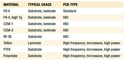
Key PCB material properties. Depending on the application, designers primarily concentrate their efforts on three basic material properties of substrates and laminates for PCBs. These are:
- Thermal properties: Tg, Td, coefficient of thermal expansion (CTE) and thermal conductivity (k)
- Electrical properties: Dk, Df, volume resistivity (⍴), and surface resistivity (⍴S)
- Chemical properties: Flammability, moisture absorption, and resistance to chemicals.
Thermal properties. The PCB material will generally face some extreme environments during its life but must retain its characteristics throughout. For instance, during stackup, a fabricator subjects the various layers of a PCB to multiple lamination cycles, where the prepreg and epoxy-glass (or other substrate material) bond under heat and pressure. Once formed and stored for some time, the PCB will be baked to drive out moisture, then is subject to reflow temperatures during assembly. In the field, the PCB can undergo operational temperature fluctuations and localized heating from hot components.
The PCB material can become soft and plastic when subjected to heat. In extreme cases, the layers can separate, an effect known as delamination. Contributing factors include temperature and the time at which the PCB material remains exposed to heat. Quickly removing the PCB material from the influence of heat can reverse the effects of softening, but the effects of delamination are more severe, often resulting in permanent damage.
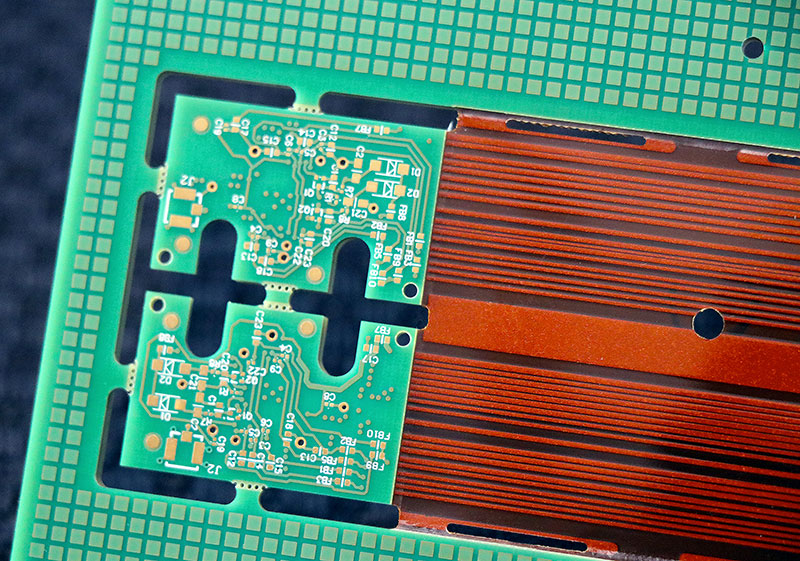
Figure 1. Board materials must retain their physical and electrical characteristics throughout the manufacturing and end-use processes.
Tg and Td. Tg denotes the threshold of temperature beyond which the material turns soft and plastic. Decomposition temperature (Td) denotes the temperature threshold beyond which the layers begin to delaminate and break down.
The most severe (elevated) temperatures a PCB faces in its lifetime are at the time of reflow. Manufacturers specify two parameters: T-260 for leaded reflow soldering and T-288 for lead-free reflow soldering. These denote the time in minutes the PCB material can withstand the peak reflow temperatures before its layers begin to deteriorate.
CTE. Allowing the temperature of an object to move away from ambient; e.g., up or down, leads to materials expanding or contracting. PCBs are no different. Indeed, the situation is more complicated, as the PCB is generally a composite of different materials that exhibit different behaviors as they transition through thermal cycles. Not only are there multiple layers of varying materials such as adhesives and laminates, but there are copper traces and layers (ground planes), and components soldered to them. Different materials expanding or contracting at different rates can spell disaster for the PCB assembly, with delamination a common result. Therefore, designers prefer to use materials that have similar CTEs in the same axes.
Thermal conductivity. When operating within the confines of an assembled product, system or piece of equipment, a PCB assembly may include components that generate heat. It is essential to remove this heat through the natural processes of conduction, convection and radiation to keep the device functioning properly. While there are more concentrated methods of heat removal through thermal vias, heatsinks and fans, the primary method is the ability of the PCB itself to remove the heat by conduction and convection. A PCB dielectric material with a suitably high thermal conductivity is essential to this ability.
Electrical properties. Depending on the application, and the speed and frequency of the signals it carries, the PCB may have to maintain high signal integrity and provide controlled impedance. Factors such as the Dk and Df of the PCB material are essential for achieving this. Low electrical leakage in the PCB material is essential in high-voltage applications, and the factors of concern here are the volume resistivity (⍴), surface resistivity (⍴S) and electrical strength across the z direction.2
Chemical properties. For safety, it is necessary for the PCB material to be flame-retardant, and it must follow UL94 or other safety standards. Moreover, as the electrical and thermal properties of PCB materials change as they retain moisture, the material must essentially have a low value for moisture absorption. PCBs are also subject to cleaning after assembly, and the PCB material selected must be resistant to these chemicals.2
Finally, the choice of the foil layer may also be an important consideration for the designer. For instance, rolled foils are commonly used for flexible circuits, while CAC is more suitable for high frequencies and HDI boards, as they offer higher density and fine-line circuits than regular foils.
References
- Tempo Automation, How to Select the Best Printed Circuit Board Material for Your Design, company website, tempoautomation.cm/blog/how-to-select-the-best-printed-circuit-board-material-for-your-design/.
- MCL, PCB Material Options and Classifications and Substrate Property Considerations, company website, Feb. 16, 2018, mclpcb.com/pcb-material-selection-guide.
Additional Reading
- Bill Hargin, “Material Selection for High-Speed PCB Design,” PCD&F, May 2019; pcdandf.com/pcdesign/index.php/editorial/menu-features/13607-high-speed-laminates-1905.
- John Coonrod, “Selecting PCB Materials for High-Frequency Applications,” EDN, Jul. 11, 2012.
- Martin Tarr, Printed Circuit Boards – Alternative Board Materials, company website, idc-online.com/technical_references/pdfs/electrical_engineering/Printed_circuit_boards_Alternative_board_materials.pdf.
- 4PCB, PCB Laminate Material Properties Guide, company website, 4pcb.com/ac-advanedtechnologymaterialsmatrix.pdf.
is chief executive of Rush PCB (rushpcb.com); roy@rushpcb.com.


Press Releases
- XLR8 EMS Welcomes Raul Jorge Lopez Jr. as Director of Program Management and Procurement
- Koh Young America Promotes Ramiro Mora to Lead Service and Applications in Mexico and South America
- ViTrox Americas Welcomes Huy Pham as Technical Support Engineer
- XLR8 EMS Appoints Steve Dutton as Chief Sales Officer