

Solder Paste Powder: When to Downsize


A finer type solder paste may solve one problem only to create another.
From Univac to the latest wearable gadget, electronics keep shrinking. As transistors get smaller, so too do their packaging, solder interconnections, and a key ingredient in making those interconnections: solder powder. Often overlooked on miniaturization roadmaps, the ultrafine particles of metal carried in solder paste play a critical role in solder joint formation, and must be optimized for printing and reflow of subminiature solder joints.
The solder powder manufacturing process is very complex and involves atomizing molten alloy and solidifying the tiny droplets while dispersed in gas. There are many different ways to atomize metallic powders. Most methods are considered proprietary and are rarely discussed in public forums. A solder paste’s flux and its attributes garner a great deal of attention. Yet the alloy powder quietly represents up to 90% of the mass of a solder paste. Understandably, solder powder can have a significant impact on every aspect of paste performance.
The highly secretive atomizing operation is considered the central step in solder powder manufacturing, but pre- and post-atomization processes are also critical factors that determine overall product quality. Pre-atomization processes include alloying, assaying and casting the metal that will be fed to the atomizer. Alloying is achieved under tightly controlled conditions in batches as large as 10 tons. Raw materials are carefully chosen for their metallic purity and oxide levels prior to mixing, and the resulting alloy is again tested afterward. Particular attention is paid to alloys containing more than three elements, alloys with dopants or trace compounds, and to preventing cross-contamination between alloys.
Once a melt is approved by quality control, it gets cast into bar stock. The bars are fed into an atomization process that heats them in a primary melting pot and transfers the molten metal into a smaller vessel. The smaller vessel pours a controlled stream of liquid solder onto a rotating disc. As the liquid hits the disc, it is deflected into droplets that are formed by surface tension into individual spheres before they freeze (FIGURE 1). Atomizing parameters include melt temperature, disc speed, chamber environment and other variables that influence key particle characteristics such as size, shape and oxide level. The relationships between input and output variables are well-guarded industry secrets.
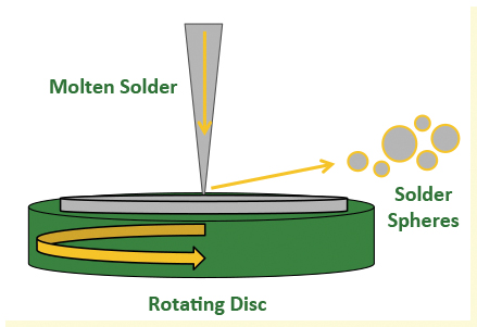
Figure 1. Solder powder atomization process.
Powder size is classified by sphere diameter (TABLE 1). Typically, atomization operations are optimized to produce a particular size powder, with spheres outside the desired range considered byproducts of the process. Spherical shapes are ideal, but sometimes irregular shapes like dog bones or tails are formed (FIGURE 2), or multiple spheres clump together. These undesired geometries can affect a solder paste’s rheology and print performance, and are removed in subsequent processing.
Table 1. JEDEC Designation of Solder Powder Types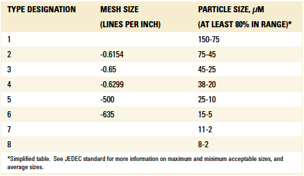
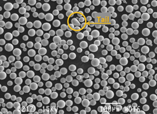
Figure 2. Type 4 solder powder with a non-spherical shape irregularity known as a “tail.”
Oxidation is controlled by manipulating levels of inert gases such as argon and nitrogen in the atomization environment. The powder’s oxide level significantly influences its overall performance on the SMT line. Because the oxide shell protects the underlying alloy from further reactions with both the environment and flux medium, a minimum amount is needed on the particles’ surfaces. But because oxides can impede the very wetting that enables solder joint formation, too much can contribute to reflow defects such as “graping” and solder balls. As sphere diameters decrease, their ratio of surface area to volume increases, amplifying the effects of the oxide shells.
Post-atomization processes include air classifying and sieving. The air classification process segregates the solder powder into different classes based on mass. The powder is blown through a stream of air or nitrogen where the target-sized particles are concentrated. The smaller sized particles are carried away in the flowing gas and the heavier particles fall into a collection area. This process permits rapid winnowing of the powder to where the most desirably sized particles are heavily concentrated. Air classifying makes the subsequent sieving operation much more efficient and effective.
Sieving sorts the classified powder using large, vibrating sieves with progressively finer screens. The screens correlate to the mesh size that defines the “type” of powder as designated by JEDEC and J-STD-005. Table 1 shows the classifications, both in terms of mesh size for the screens and resulting particle sizes.
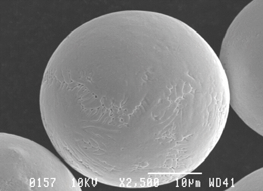
Figure 3. A 35µm diameter solder powder particle.
Spheres categorized as Type 3, or T3, will fall through a 325 mesh screen but not through a 500 mesh screen, hence the term -325+500. This equates to particle sizes of 25 to 45µm; 80% of the particles must meet this size requirement. Likewise, Type 4 paste will fall through a 400 mesh screen but not a 635 mesh screen, equating to particle sizes of 20 to 38µm. There is a lot of size overlap between the T3 and T4 classes; therefore, T4 solder paste can typically offer a slight edge in fine feature printing without presenting substantial reflow concerns. Particle size drops off quickly at Type 5 to 10 to 25µm, however, and while the solder paste’s fine feature print capability is dramatically improved, the effects of the surface oxides can start to factor in; shelf life may be affected, and the potential for reflow coalescence problems are increased.
For decades, Type 3 solder paste dominated SMT assembly. Because most solder powder operations were optimized to produce Type 3, Type 4 pastes commanded a price premium. That is no longer the case; demand for T4 has increased, and atomizing technology has become more agile, driving the two powder types’ cost parity. Today’s Type 3 and 4 pastes are capable of easily printing and reflowing component sizes down to 0.5mm BGAs and 0201s. A 10-year-old solder paste formulation from the early Pb-free days might not be capable, but a modern product that uses current flux chemistries and high-quality solder powder certainly can – and does – do the job very well.
When fine features present printing problems, it’s only natural to seek out a finer type solder paste, which can sometimes provide a quick fix. Unfortunately, it’s not always the best remedy, as it may serve to resolve one set of process issues but create others. A switch from T3 or T4 to a T5 will print better, but potentially at the cost of unwanted solder balls or graping. When facing printing problems with features of 10 mils (0.25mm) diameter or larger, the most effective approach is to audit the process itself to ensure it is stable and optimized. Check tooling setups; use quality stencils with flux-repellent nanocoatings; verify solvent-paste compatibility, and dial in the print parameters with a simple experiment. Ask advice from your solder paste and stencil providers; they respond to problems like these on a daily basis and have many answers at the ready. Plus, many paste suppliers can help with process audits. If a move to a finer powder or improved stencil technology is warranted, your supplier should let you know.
Wearable, portable or implantable miniaturized devices with 0.4mm or smaller arrays and 01005s absolutely require finer powder solder pastes (and sometimes specialized fluxes), but for the vast majority of SMT applications out there, off-the-shelf Type 3 or 4 is still the best bet, with T4 rapidly becoming the default on new paste products. These types are readily available, robust and reliable, and will continue to be the most produced and consumed types of solder paste on the market for years to come.
is regional manager at AIM; toneill@aimsolder.com. is vice president of technology at AIM Solder; kseelig@aimsolder.com.


Press Releases
- Javad EMS Upgrades Through-Hole Soldering Capacity with New SEHO PowerWave System
- Sharpen Your Selective Soldering Skills with Kurtz Ersa's July VERSAFLOW 4/55 Training
- Omron Advances Inspection Technology with NVIDIA Omniverse and Metropolis
- Seika Machinery’s SMI 2026 Webinar Series Continues with Focus on PCB Cleaning Before Solder Paste Printing