

Locating BGA Joint Failures

Why “dye and pry” is a fast, workable solution.
This month we show examples of testing BGAs with a “dye and pry,” a simple and cost-effective way of looking at joint failure or their condition after some form of mechanical testing or abnormal assembly practice.
FIGURE 1 shows a sample BGA joint after dye-and-pry testing. Eighty percent of the separated surface is covered by the red dye. This clearly shows separation occurred before the dye was added.
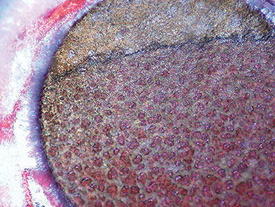
Figure 1. Sample BGA joint after dye-and-pry testing.
FIGURE 2 shows a solder ball separated from the pad on the PCB. There is no evidence of dye present. This indicates no cracks were present before the two surfaces were separated. The image also shows how the solder has formed around the pad during reflow like an upturned plate.
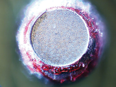
Figure 2. A solder ball separated from the pad on a PCB.
Some engineers feel “pry” is a bad method, but it’s all about the care used when selecting or performing this test. It can take a few minutes to test parts, so quick results can be obtained in production settings, rather than spending hours in a lab. For those who have been trained correctly, it’s not as difficult as some suggest.
We have presented live process defect clinics at exhibitions all over the world. Many of our Defect of the Month videos are available online at youtube.com/user/mrbobwillis.
is a process engineering consultant; bob@bobwillis.co.uk. His column appears monthly.


Press Releases
- ViTrox Americas Welcomes Doug Ennis as Senior Field Applications & Service Engineer
- Altus Adds LPKF CuttingMaster 3290 to Depaneling Portfolio
- Kurtz Ersa Partners with E-tronix for Sales in Illinois and Wisconsin
- XLR8 EMS Welcomes Raul Jorge Lopez Jr. as Director of Program Management and Procurement