

Investigating the Metric 0201 Assembly Process
The feasibility of high-volume microminiature component manufacturing using Type 5 and 6 pastes.
The introduction of metric 0201 components into high-volume mobile communications products is causing the surface mount technology (SMT) community to ask how this will affect the assembly process. The three main elements of SMT are printing, placement and reflow. This article investigates each element.
Within the printing process, a stencil thickness of 60µm will be used. This foil thickness is the minimum compatible with the heterogeneous requirements for the mobile communications sector. To obtain a comprehensive understanding of the process window associated with the assembly process of metric 0201, two solder paste materials were evaluated, along with three component interspaces and two pad designs. The solder paste materials have two different grain sizes, while the pad designs include two different footprints and three pad-to-pad interspace dimensions.
Experiment
The supplier, input, process, output and customer (SIPOC) diagram (FIGURE 1) outlines the methodology used in the investigation.
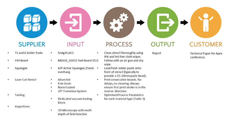
Figure 1. SIPOC flow chart.
Aperture design and area ratio. TABLE 1 outlines the aperture design and associated area ratios. To accommodate the required 60µm stencil foil, the area ratio violates IPC-7525 guidelines.
Table 1. Aperture Designs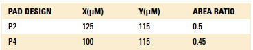
Board design. The printed circuit board (PCB) was manufactured from FR-4 with a gold-over-nickel finish. The PCB dimensions were 200mm x 150mm with a board thickness of 1mm. Due to fabrication limitations, solder mask is not present within the pad areas. Pad designs used throughout the investigation are shown in FIGURE 2. Both pad designs have an interspace of 50µm, 75µm and 100µm. Each design has 80 replicates. The P2 pad design includes a trace 60µm wide; this is not present on the P4 design.
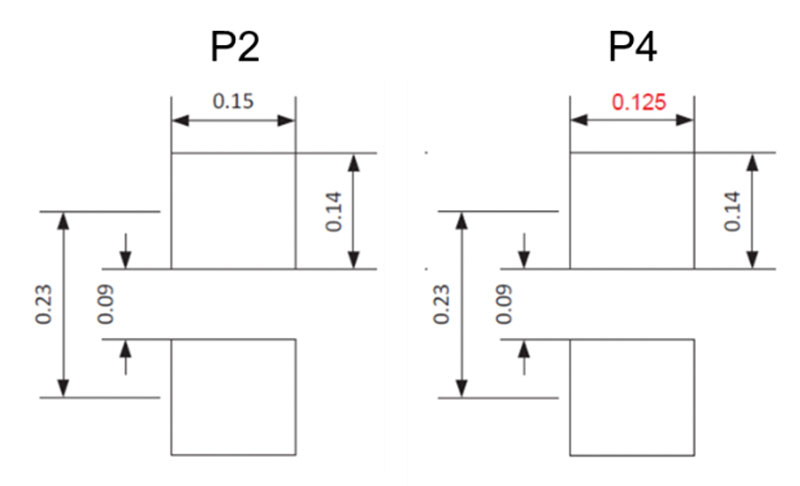
Figure 2. Pad dimensions (mm).
Material set. The stencil technology used throughout the investigation was a fine-grain stainless steel with nanocoating applied to the board plane. The stencil foil was fabricated using a diode-pulsed laser-cutting machine and mounted into a frameless system. Type 5 and 6 solder paste materials were used within the investigation, and all materials are commercially available. Each solder paste material was optimized for printing; these process parameters can be seen in TABLE 2.
Table 2. Solder Paste Printing Parameters
Print to destruction. To understand the print capabilities of each material, a print-to-destruction test was performed on both solder paste materials. This test will aid in understanding the print capability and working window of each material. Each material was printed using a 14-board run with no under-stencil cleaning. The fifth and last board were contrasted and compared against process stability.
FIGURES 3 and 4 show the print quality achieved for both solder paste material types. For simplicity, only the 50µm P4 design is shown. Figures 3 and 4 show the Type 5 material produced a fuller print deposit. This fuller print created a propensity to create solder paste bridging. This was observed from the fifth board onward on both pad designs for the 50µm interspace. The Type 5 solder paste material printed with a higher definition; however, solder paste bridging was also observed on the 14th board for the P2 design and 50µm interspace. Although both solder paste materials created bridge defects with the 50µm interspace, the Type 6 had a higher propensity to create process defects. Therefore, it can be concluded a Type 5 solder paste material has a higher wet printing capability than the finer grain Type 6 material.
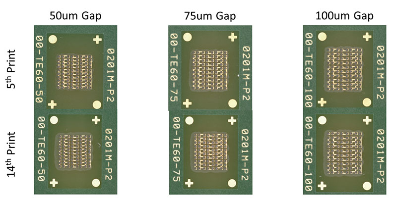
Figure 3. Type 5 solder paste P2 pad design print to destruction.
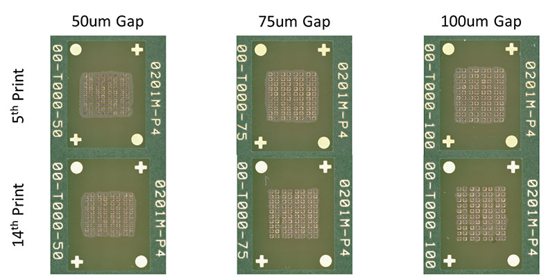
Figure 4. Type 5 solder paste P4 pad design print to destruction.
The next step of the investigation is to assemble the metric 0201 board.
Metric 0201 assembly. Assembly trials used the following equipment: a fully automatic stencil printer capable of 12.5µm alignments at 2 Cpk; an automated placement machine with a multi-station high-speed placement head with a high-resolution vision system; a multi-programmable zone reflow oven with nitrogen capability. For all the assembly runs, the optimized print parameters (Table 2) were used. To ensure the printing process had stabilized, four test boards were processed before running two production boards; the second production board was used for the analysis.
Results/Analysis
Figures 7 to 16 show the findings from the assembly trial. Both solder paste materials and pad designs P2 and P4 are shown. To maintain a certeris paribus methodology the same location of the PCB is displayed for each process step, thus permitting the process to be chronologically recorded.
FIGURES 5a to 7a display the printing results from the Type 5 solder paste material and three interspace P4 pad designs. Visually, the paste printing process shows some variation; however, the printing process generally meets all inspection standards. The observed variation is a result of the apertures associated to area ratio of 0.45. This value falls outside the IPC minimum recommendation of 0.5 or greater, per IPC-7525. Figures 5b to 7b show the metric 0201 after placement. Visually, the placement of the metric 0201 components look acceptable with no missing or skewed parts. Also worth noticing, the placement process has not compressed/bridged the solder paste material. Finally, Figures 5c to 7c show the P4 pad designs after reflow. The solder joint integrity visually looks acceptable with no dry or bridged joints.
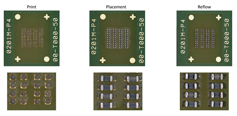
Figure 5. Print P4 type 5 (a), placement (b) and reflow (c); 50µm interspace.
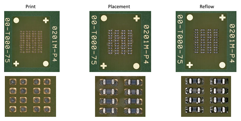
Figure 6. Print P4 type 5 (a), placement (b) and (c) reflow; 75µm interspace.
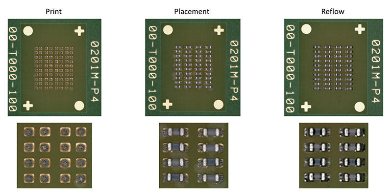
Figure 7. Print P4 type 5 (a), placement (b) and reflow (c); 100µm interspace.
FIGURES 8a to 10a show the printing results from the Type 5 solder paste material and three interspace P2 pad designs. The P2 pad design has an end trace of 60µm. The paste printing process meets the visual requirements of repeatable/present deposits. The area ratio associated with the P2 design is 0.5. This is at the extremities of the allowable value, as prescribed by IPC-7525. Figures 8b to 10b show the metric 0201 after placement. Visually, the placement of the devices looks acceptable, with no missing or skewed parts. As this pad design has an end trace, it is worth noticing the solder paste material has not been compressed by the placement process, such that the fluid elements of the material have bled across the track elements. Finally, Figures 8c to 10c show the P2 pad designs after reflow. Solder joint integrity visually looks acceptable with no dry or bridging joints. The solder paste has flowed across the conjoined traces, but wetting forces have not modified the original placement position of the metric 0201 devices.
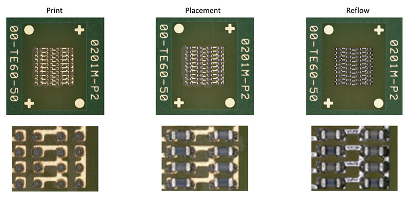
Figure 8. Print P2 type 5 (a), placement (b) and reflow (c); 50µm interspace.
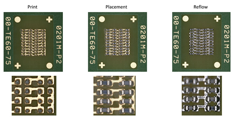
Figure 9. Print P2 type 5 (a), placement (b) and reflow (c); 75µm interspace.
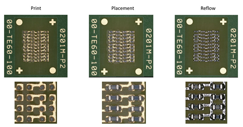
Figure 10. Print P2 type 5 (a), placement (b), and reflow (c); 100µm interspace.
FIGURES 11a to 13a show printing results from the Type 6 solder paste material with the P4 designs and associated interspaces. The Type 6 solder paste material produces a fuller print. This is caused by the Type 6 material’s finer particle size. Although the print is fuller than the Type 5 solder paste material, the variation of deposit to deposit has not significantly improved. Figures 11b to 13b show the metric 0201 component after placement. The 50µm interspace examples have been compressed to a point where the solder paste material has abutted to an adjacent pad. The 75µm and 100µm interspace examples also exhibit the same observation, but due to the increased distance from pad to pad, the propensity to bridge has diminished. Figures 11c to 13c show the P4 examples after the reflow process. Worth noticing is the 50µm interspace examples have not culminated in bridged interconnects.
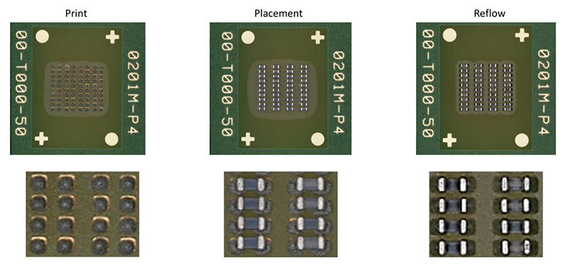
Figure 11. Print P2 type 6 (a), placement (b) and reflow (c); 50µm interspace.
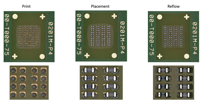
Figure 12. Print P2 type 6 (a), placement and reflow (c); 75µm interspace.
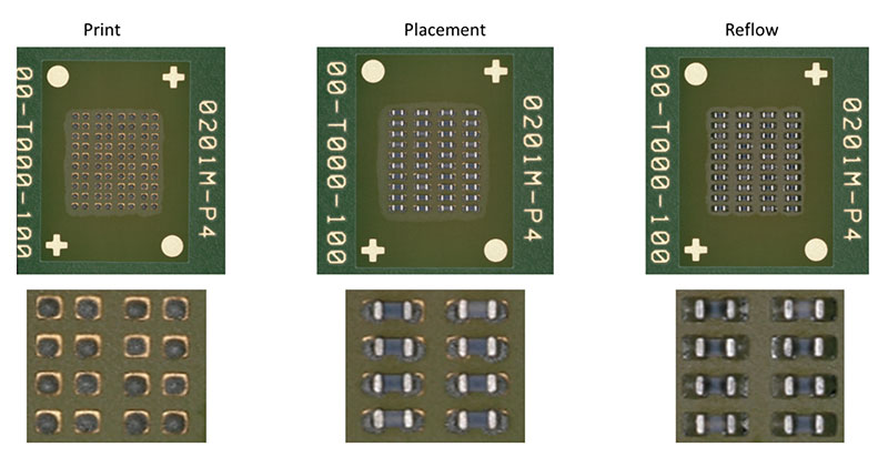
Figure 13. Print P2 type 6 (a), placement (b) and reflow (c); 100µm interspace.
FIGURES 14a to 16a show the print quality from the P2 pad design using Type 6 solder paste. As with the P4 examples, the Type 6 material produced a fuller print than the Type 5 material. Again, the fuller deposits are increasing the propensity to bridge. Figures 14b to 16b show the metric 0201 component after placement. The 50µm interspace examples have been compressed to a point where the solder paste material has abutted to an adjacent pad. The 75µm and 100µm interspace examples also exhibit the same tendency, but due to the increased distance from pad to pad, the propensity to bridge has diminished. Figures 14c to 16c show the P2 designs after reflow. The 50µm and 75µm interspaced examples have numerous instances of conjoined interconnects. The solder joints that have bridged are all associated with traces that adjoin neighboring pads. Therefore, electrically the interconnect meets the design requirements. From a manufacturing standards perspective, however, the conjoined devices do not meet quality standards and therefore would not be fit for purpose.
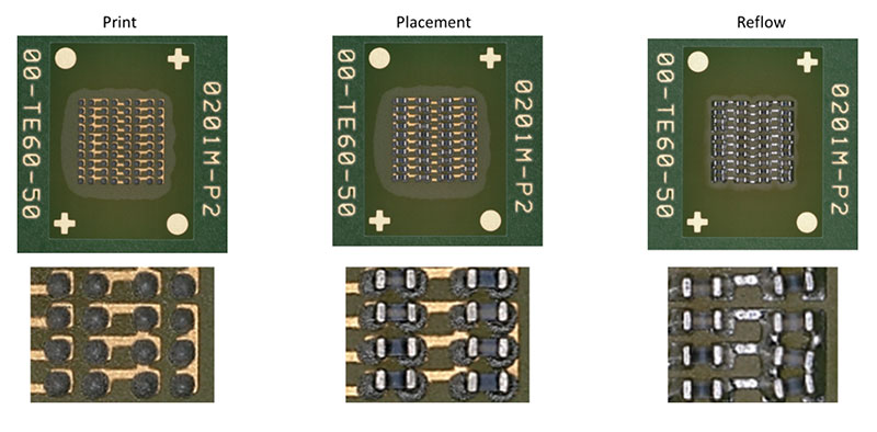
Figure 14. Print P2 type 6 (a), placement (b) and reflow (c); 50µm interspace.
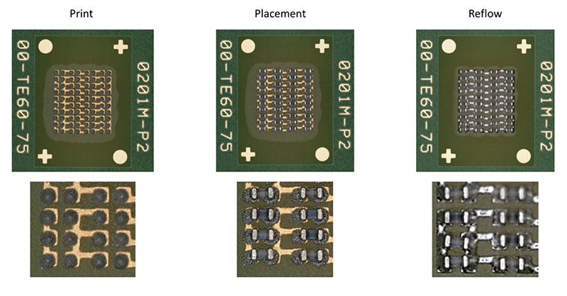
Figure 15. Print P2 type 6 (a); placement (b) and reflow (c); 75µm interspace.
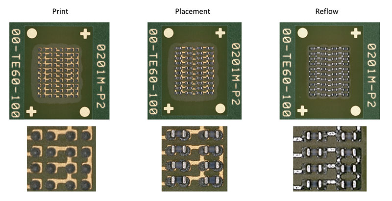
Figure 16. Print P2 type 6 (a), placement (b) and reflow (c); 100µm interspace.
Conclusions
This investigation led to several findings. Industry guidelines and general rules-of-thumb claim a finer particle paste will produce an enhanced print quality. However, it has been observed through this investigation that although a finer grain Type 6 solder paste material has produced a fuller print deposit for both pad designs, the resultant process capability has not followed this prediction. The printing and placement processes have been negatively affected by the inclusion of excessive solder paste volume.
Within the printing process, the excessive volume has caused the solder paste to saturate its designed area, thus causing the solder paste to merge into a neighboring region. Within the placement process, an excessive volume of solder paste caused the pressure of placement to squeeze out the solder paste beneath the component’s termination. In the interspace examples of 50µm and 75µm, this deformation of solder paste caused enough movement to form a solder paste bridge.
The Type 5 solder paste was not exempt from process issues, and the variation between deposits was still observed. However, the volume of solder paste was compatible with the application of metric 0201 assembly. The main observation was a reduction of bridging errors on the finer interspaces. The inclusion of a conjoined trace (P2 design) also added an additional challenge to the investigation. The trace provides a path for the liquid elements of the printed solder paste and reflowed molten solder to migrate. The increased volume produced by the finer grain Type 6 solder paste material resulted in an increased propensity of bridging along the traces from both the printing and reflow processes. The additional issue with reflow-generated bridging is the tendency for the molten solder to alter the position of components. This is due to the surface tension of molten solder overcoming the mass of the metric 0201 component. The lower volume delivered by the Type 5 solder paste material produced less solder paste and reflowed bridging.
Within this investigation, assembly of metric 0201 components has been accomplished with area ratios as low as 0.45, interspaces down to 50µm, a 60µm conjoined trace, and pad dimensions of 100µm x 115µm. The material selection for successful metric 0201 assembly is as follows: 60µm fine-grain stainless steel foil with a polymer coating and Type 5 grain-sized solder paste.
Ed.: This paper was originally published at IPC Apex Expo in January 2019 and is reprinted here with the author’s permission.
is global applied process engineering manager at ASM Assembly Systems, Printing Solutions Division (asmpt.com); clive.ashmore@asmpt.com.


