


Hints for offsetting QFN void formation.
QFNs: Designers love them. Assemblers don’t necessarily share that affection. These very popular devices, first on the electronics scene in the late 90s/early 2000s, have become one of the more popular packages among handheld manufacturers. From a design and manufacturing point of view, the QFN is an excellent package. QFNs are flat, plastic packages with perimeter leads underneath the device (as opposed to leads that extend outside the package) with a large pad in the center. They are low-cost in comparison to other components, allow a high number of I/Os and are an excellent alternative to traditional QFPs, TSOPs and the like.
A QFN’s ability to pack major functionality into a relatively thin package in addition to excellent electrical and thermal performance has driven their popularity. And, since their introduction over a decade ago, these devices have expanded on their functionality capability. Advancement in QFN design has given rise to dual- and even triple-row perimeter I/O, whereas the first designs had only a single perimeter row of I/O. In addition, QFNs are now incorporating other packaging styles such as internal die stacking to increase function.
So, while designers adore the QFN for all of the design latitude, assembly specialists – and to some degree packaging specialists – have many QFN challenges to overcome. At the package level, manufacturing hurdles include issues with wire bonding on polyimide and the die to pad ratio effect on JEDEC performance. New conductive die attach films, however, are helping overcome the die to pad ratio challenge and are also enabling more die per package, as these materials essentially eliminate the fillet associated with paste-based mediums. At the board level, ensuring long-term reliability is the central issue. In truth, what makes the QFN so appealing for component and handheld product designers is at the root of one of its greatest assembly challenges: solder voiding.
The architecture of the QFN makes it inherently more susceptible to void formation. The reduced standoff (which makes these components appealing to designers) combined with the planar surfaces easily traps escaping solvent vapors and activator residues. While the increased cross-section of the interconnect joints compared with a CSP mean that voiding is typically not a reliability issue, the same cannot be said of the central ground plane which is often used as a heat sink. The large central solder paste deposit provides only very limited escape routes for the volatile materials generated during a reflow process, resulting in an increased level of voiding.
The parameters that contribute to QFN voiding are many and varied including the size and design of the device itself, reflow profiles, solder paste capability and multiple other process conditions. And, just as there are multiple factors influencing the formation of QFN voids, there are several approaches to reducing them. One of the more well-established techniques for minimizing voiding is depositing the paste for the center pad in a specific pattern, depending on the size of the QFN. Arguably the most popular of these is the windowpane pattern where the pad is divided into between four and 16 equally-sized smaller deposits (Figure 1). Although these patterns are well-used, little work has been done on the efficacy of any one design. The ratio of total pad area to deposit area becomes more important as the number of panes increases and it is crucial not to starve the pad of solder as this can cause an increase in voiding. This approach can reduce the voiding from around 35% for a single large deposit down to below 20%.

The paste pattern is important, but even more critical is a complete understanding of the characteristics and capability of the flux medium formulation within the solder paste and, to some degree, the alloy construction. Partnering with a materials supplier that has expertise in flux development and can test flux performance in-process prior to material commercialization ensures success. Over the past few years, major advances in flux formulation technology have been achieved and this evolution in flux design is benefitting QFNs and other large planar pad devices in terms of overall performance – including the reduction of voids.
The simple fact is that a complete understanding of the role and interaction of the various flux components and their ultimate impact on the performance of the final paste is essential to optimize product performance. A supplier’s formulation expertise and application knowledge regarding the acids, bases, rosins, activators, alloys and other flux components enables the development of high performance fluxes and solder pastes. In fact, newer generation solder pastes have shown as much as a 10% to 15% reduction in the base QFN voiding as compared to older generation pastes and this is due in large part to the evolution of flux design techniques. That said, each process, each environment and each assembly is unique and, therefore, takes a customized approach to delivering high yields and high reliability. It’s not only flux formulations that impact voiding; it’s also other paste characteristics such as rheology during reflow that enable voids to escape more easily.
There are multiple factors that affect QFN void formation including the flux, alloy, reflow, component type and board metallization, to name a few. Without question, flux is a huge variable when it comes to voids but it has to be balanced with all of the other factors as well. My advice? Start with robust flux formulations, understand each customer’s unique process conditions, delve into the specific application and then develop a solution that achieves the desired QFN result: less voids and higher reliability.
Acknowledgements
The author would like to thank technical service supervisor Jonathan Jiang of Henkel for his valuable input.
Jie Bai is a chemist at Henkel Electronics Group (henkel.com); jie.bai@us.henkel.com.
Why one solvents expert thinks we have the method for approving substances backwards.
The popular solvent known as 1-bromopropane (aka n-propyl bromide or nPB for short) came on the industrial market in 1996. Its main uses are metal cleaning, diluent for adhesives, dry-cleaning garments, and – most relevant to readers – defluxing electronics assemblies.
When it was first marketed, there were no data on toxicity, carcinogenicity, mutagenicity, and so on. The makers initially proposed a 500ppm limit of the substance in the air breathed by workers, but this was rapidly dropped to 200ppm. This was the Operator Exposure Limit (OEL), and it was only a recommendation. One small French producer recommended 10ppm. The US National Toxicity Program started work on it in the early 2000s, but this is still ongoing. OSHA cannot issue a permitted legal limit (PEL) until the NTP has finished. In the early 2000s, anecdotal reports started coming out, indicating neurological problems in some workers exposed to the substance. The makers funded some animal tests, and most of them dropped their recommendations to 100ppm in the mid-2000s after it was found that mice suffered longer nerve reactions in the CNS and lower sperm motility. Later results indicated that both the neurotoxicity and the reproductive toxicity were worse than thought, and most makers reduced their recommended OEL to 25ppm, although one recommended 100ppm. This is still valid today.
From the practical point of view, 100ppm is fairly easy to control. The limit of possible for defluxing in our industry is 25ppm using ordinary high-quality open-top machines. So-called “zero-emission” machines are available but cost three to five times more than conventional ones and generally can hold average exposure to lower single digits if used correctly.
In Europe, nPB was classed as a VOC (less regulated in the US), and the VOC Directive limited its use to negligible amounts. However, the REACH program has proposed labeling it as a reproductive toxin, but this has not yet been studied. In China, where vast amounts are made and used, the limit is pending.
About two years ago, the NTP issued an interim warning that animal tests on both rats and mice indicated a strong probability of carcinogenicity and mutagenicity. The American Conference of Government and Industrial Hygienists (ACGIH) issued a Threshold Limit Value (TLV), similar to the OEL, of 10ppm. The ACGIH is a highly respected NGO, and its recommendations are based on known science, but it has no force of law. However, many companies using chemicals do try to take notice of its recommendations.
The ACGIH has recently put a cat among the pigeons in that it has given advanced notice of a change in the TLV for nPB. The proposed draft value is 0.1ppm, an unprecedented two whole orders of magnitude lower than the current TLV (acgih.org/store/ProductDetail.cfm?id=2151). I’m not yet aware of the reason behind this, but it must be serious.
Needless to say, 0.1ppm is impossible to respect under industrial conditions so, if this value were to become a legal limit, nPB would be condemned to death as an industrial solvent for defluxing, etc. (It is also used in small quantities as feedstock for the pharma industry in the manufacture of psychotropic drugs such as diazepam.)
Why this rant? Simply because I suggest we have it wrong, all wrong. Workers were initially exposed to what has been deemed potentially dangerous levels of nPB, up to 5,000 times higher than the proposed “safe limit.” Even today, one maker is recommending an OEL of 1,000 times the proposed OEL. This is far from the first time that workers have been told that such-and-such a chemical is safe, only to die prematurely from the effects of exposure 10, 20 or 30 years later; I know of cases, one involving a close friend, where people have died in their 50s and 60s from organ failures resulting from chemical exposure as young adults.
Yes, we say that chemicals are innocent until proven guilty. This is wrong, and I suggest that they should be considered guilty unless proven innocent. An arbitrary tight limit should be placed on new chemicals, based on computer modeling and analogical comparison with similar known substances. This limit may be slackened if tests and experience show it is safe to do so.
Brian Ellis is a retired consultant and longtime vice-chairman of the IPC Cleaning Handbook task group. He is author of Cleaning and Contamination of Electronics Components and Assemblies, among several other books and technical papers. He was a member on the Solvents Technical Options Committee of UNEP, advisory to the Parties of the Montreal Protocol, from 1989 to 2004, co-chaired the nPB Task Force and was Senior Solvents Consultant to the UNEP Multilateral Fund and to the Swiss Federal Office of the Environment. He founded Protonique SA and Protonique Ltd. and developed the Contaminometer, the Insulohmeter, the APL series of aqueous cleaners and driers and other equipment; bne@bnellis.eu.
Used properly, standards can be effective tools in a static control program.
Economic pressures, device densities, new technologies, and an increased reliance on outsourcing are just a few of the ongoing indicators of change in electronics production. And ESD control has a key role in coping with some of these changes facing the industry.
In meeting the complex challenge of reducing ESD losses, standards are playing an increasing role in reducing marketplace confusion in the manufacture, evaluation, selection of static control products and implementation of static control programs. Standards help to ensure lot-to-lot consistency for static control products and provide a means of objective evaluation and comparison among competitive ESD control products. Standards help reduce conflicts between users and suppliers of ESD control products and are used in developing, implementing, auditing, and certifying ESD control programs.
Standards, however, should be viewed simply as tools, and like any tool, effectiveness is often a function of how well the tool is used. When properly used to drive a nail, a hammer ensures that siding adheres to the frame of a house. A swollen thumb is vivid testimony to the hammer’s misuse. Current industry conditions demand that all available tools be put to good use. Wasting time and money is out of the question. The following is a set of guidelines for effective use of standards.
First, evaluate and select standards that are appropriate for your specific applications. In the US, use of standards is generally voluntary, although their use may be written into contracts or purchasing agreements between a buyer and seller. In much of the rest of the world, the use of standards is usually compulsory, and they often have the force of law behind them. Manufacturers should carefully consider and make the right decision when given the option to use, or not use, standards. Good decisions are based on good information and analysis of need. Use those standards applicable to your manufacturing environment, and confusion will be greatly reduced and efficiency will improve.
Second, understand the difference between a standard and a test method, and use each accordingly. The term “standard” is often used to refer to all standards-related documents, but significant differences exist in the different types of documents. A true standard is a precise statement of a set of requirements to be satisfied by a material, product, system or process: the electrical resistance of a worksurface, for example.
Usually, a standards document also specifies the procedures (test methods) for determining whether each of the requirements is satisfied. For instance, you can specify that the worksurfaces in your facility meet the requirements outlined in a standard.
A test method is a definitive procedure for the identification, measurement and evaluation of one or more qualities, characteristics or properties of a material, product, system or process. For example, you can specify that the worksurfaces have a specific resistance level when measured according to the test method, but you cannot specify that the worksurfaces meet the requirements of the test method, because the test method normally doesn’t contain the actual specification for the product being tested.
You’ll avoid a lot of conflicts in purchasing and in program implementation when you use the right type of document for the specific application.
Third, understand what the standard covers and what it doesn’t. Usually this type of information is found in the scope of the document. If the scope says the document covers worksurfaces with a resistance to ground of 106-109Ω, then the document is not applicable for materials requiring 1010Ω or more. If the scope indicates the document applies to facilities that manufacture explosives, then it may not be applicable to facilities that manufacture semiconductor devices. A thorough understanding of the document’s scope will prevent the purchase of incompatible products and the implementation of a faulty manufacturing procedure.
Fourth, learn the detailed provisions of the standard. If the document specifies resistance, then you would not select a material based on its resistivity. If the test method specifies the application of 100V when measuring resistance, you may need to replace your resistance meter that applies 500V.
Finally, be specific and clear in all communications. If a potential material supplier provides confusing specifications, ask questions and get clarification. If evaluating materials using a specific test method, reference that test method correctly in program documentation. And, always make sure to include appropriate staff in communications: vendors, customers, production managers, and the purchasing department.
Used properly, standards can be important and effective tools in your static control program.
This column is written by The ESD Association (esda.org); info@esda.org.
LEDs
“Understanding Power LED Lifetime Analysis”
Author: Philips Lumileds Lighting
Abstract: When designing LED-based lighting systems, engineers need to understand LED lumen maintenance and mortality in similar terms to those used when designing with conventional light sources. However, comparable data have been nearly impossible to find. In addition, designers need extra information to predict the lifetime of LEDs under a variety of operating conditions. A number of techniques to predict LED lifetimes have been proposed, but have not been sufficient to generate the clear and unambiguous data that lighting engineers can use easily. A new tool from Philips simplifies the process, allowing full flexibility in design options. This one tool provides information for making decisions about product lifetimes, driver constraints, number of LEDs required, and thermal management. (Company white paper)
Signal Integrity
“Bandwidth Tests Reveal Shrinking Eye Diagrams and Signal Integrity Problems”
Authors: Tim Caffee and Eric Johnson; ejohnson@asset-intertech.com.
Abstract: Each new generation of a high-speed bus typically runs at a higher signal frequency, but this decreases the margin for error on the bus, making it more sensitive to disruptions from jitter, inter-symbol interference (ISI), crosstalk and other factors. To avoid potential problems on high-speed buses like DDR3, PCI Express, Intel QPI, Serial ATA, USB and others, bus performance must be validated during each phase of a system’s lifecycle, including design/development, manufacturing and as an installed system in the field. Unfortunately, effectively and economically validating the signal integrity on a high-speed bus has become more difficult, as the limitations of legacy probe-based test equipment such as oscilloscopes have become more obvious in recent years. Non-intrusive software-driven test methods based on embedded instrumentation are providing alternative validation solutions that are more cost-effective and deliver observed signal integrity data. (Company white paper, November 2012)
Solder Joint Reliability
“The Role of Pd in Sn-Ag-Cu Solder Interconnect Mechanical Shock Performance”
Authors: Tae-Kyu Lee, Ph.D., Bite Zhou, Thomas R. Bieler, Chien-Fu Tseng and Jeng-Gong Duh; taeklee@cisco.com.
Abstract: The mechanical stability of solder joints with Pd added to SnAgCu alloy with different aging conditions was investigated in a high-G level shock environment. A test vehicle with three different strain and shock level conditions in one board was used to identify the joint stability and failure modes. The results revealed that Pd provided stability at the package-side interface with an overall shock performance improvement of over 65% compared with the SnAgCu alloy without Pd. A dependency on the pad structure was also identified. However, the strengthening mechanism was only observed in the non-solder mask-defined pad design, whereas the solder mask-defined pad design boards showed no improvement in shock performance with Pd-added solders. The effects of Sn grain orientation on shock performance, interconnect stability, and crack propagation path with and without Pd are discussed. SAC 305 + Pd solder joints showed more grain refinements, recrystallization, and especially mechanical twin deformation during the shock test, which provides a partial explanation for the ability of SAC 305 + Pd to absorb more shock-induced energy through active deformation compared with SAC 305. (Journal of Electronic Materials, December 2012)
“A Mechanistically Justified Model for Life of SnAgCu Solder Joints in Thermal Cycling”
Authors: Peter Borgesen, Ph.D., Linlin Yang, Awni Qasaimeh, Babak Arfaei, Liang Yin, Michael Meilunas, and Martin Anselm; pborgese@binghamton.edu.
Abstract: We have shown the life of a SAC solder joint in a typical BGA or CSP assembly in thermal cycling to scale with the time to completion of a network of high angle grain boundaries across the high strain region of the joint. This provides for a scientifically credible materials science-based model. In-depth studies did, however, show this to require significant temperature variations. Isothermal cycling may also lead to recrystallization, albeit at a much lower level depending on alloy, processes, and cycling parameters, but a quantitative model would need to be completely different. The question therefore arises as to how large a cycling temperature range is required for our model to apply. We present results indicating that repeated cycling between 20˚ and 60˚C should be sufficient; i.e., the model should permit extrapolation of accelerated test results to realistic service conditions. Many practical applications involve a combination of thermal excursions and mechanical cycling, and there is little doubt that thermal cycling-induced recrystallization will tend to lead to much faster crack growth through the solder in subsequent vibration, etc. (SMTA Pan Pac Symposium, January 2013)
This column provides abstracts from recent industry conferences and company white papers. Our goal is to provide an added opportunity for readers to keep abreast of technology and business trends.
A review of four case studies of product conversions.
With the next RoHS compliance deadline approaching in July 2014, many electronics manufacturers that were exempted from the 2006 mandate will soon be forced to comply.
The initial conversion of consumer and other electronics was painful and costly at all levels of the supply chain. But over the past six years, many valuable lessons have been learned that can ease the transition for the next wave of products pursuing compliance. Furthermore, the higher reliability products with longer lifecycles typically use older packaging and PCB technology, and therefore are excellent candidates for cost reductions as their designs are updated.
Keys to a successful, economically advantageous conversion include thoroughly reviewing the product’s design, identification of cost-reduction opportunities and allotting adequate time for testing and qualification.
The first step in any RoHS conversion activity is a thorough analysis of the product’s bill of materials (BoM). The BoM should be reviewed, or “scrubbed,” for availability of RoHS-compliant components, for compliant components that are or will soon become obsolete, and for opportunities to transition through-hole (PTH) component to surface mount (SMT).
The BoM scrub will indicate one of three situations:
1. Complete set of RoHS-compliant parts are available.
2. Some parts are not available as RoHS compliant.
3. Some parts are not available as RoHS compliant, and others face obsolescence issues.
Each scenario requires different actions to complete the product conversion.
If a complete set of RoHS-compliant components is available, the conversion is very straightforward and relatively easy. The BoM is updated, and a design for manufacture (DfM) review is conducted. The primary purpose of the DfM review in this situation is to update the land patterns for Pb-free processing using the original PCB layout. The layout is updated to reflect the new footprints and, whenever possible, incorporate other DfM opportunities identified in the review. After the layout is updated, the fab drawing is then updated to indicate the new RoHS-compliant material and process requirements.
The product with the updated BoM, layout and fabrication drawing gets prototyped, tested and validated using standard manufacturing processes and practices. Following validation of the compliant product, final documentation is prepared and production is started. With the fully RoHS-compliant assembly now in production, the conversion process is considered complete.
If a complete set of RoHS-compliant parts is not available, the process requires several extra steps that take a little more time and cost a little more money. Alternate components must be researched, selected and approved. In some cases multiple parts may be required to satisfy the functional requirements of the unavailable components. A new BoM must be generated, and when complete, a DfM review is conducted. Because the new BoM will likely require a new PCB layout, more DfM opportunities may be incorporated during the re-layout phase. The new PCB design will dictate a new fabrication documentation package.
With the added steps of identifying new components and the new PCB layout complete, the conversion process now follows the same path as the product with simpler updates. It is prototyped, tested and validated. Then the final documentation is prepared, production is launched, and the conversion is finalized.
If a complete set of RoHS-compliant parts is not available and component maturity or obsolescence issues signal the need for redesign, the conversion process again requires more added steps, time and cost. Alternate components are identified, a new BoM is generated, and a DfM review is conducted. However, eliminating the antiquated or obsolete components may require major mechanical, electrical or electronic redesign. The new design will also need a complete new set of documentation.
As with the other two conversion situations, the design now progresses through the same prototype, test and validation phases; the final documentation is prepared; production is begun, and the process is completed.
Figure 1 depicts the RoHS conversion process and outlines the key engineering activity in the green boxes. Every conversion starts with a thorough BoM scrub. This is arguably the most important part of the conversion process, as its results determine the conversion path. Failure to identify exact drop-in replacements or impending obsolescence issues at the earliest stage can result in expensive setbacks and course corrections at later stages of the project.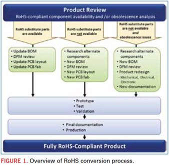
Every conversion concludes with the same activities: prototyping, testing, validating, documenting and producing. Depending on the end-use of the product, testing and validating times can vary dramatically. When planning to meet conversion deadlines, validation requirements should be carefully considered.
In between the BoM scrub and the prototype build, a lot of engineering takes place. The following four case studies describe the key engineering activity in each conversion process.
Case 1: Remote display keypad for medical device. Figure 2 shows before and after images of a medical manufacturer’s device user interface module. This is an example of an extremely simple RoHS conversion. The BoM scrub indicated that all but one part was available in Pb-free surface finish, and the one missing component was easy to replace. The scrub also identified a major cost reduction opportunity: updating the PTH transistors to SMT packages. The SMT components are less expensive than the PTH ones, and the SMT assembly process is far more cost-efficient than PTH assembly. The new components fit within the footprints of the previous components, so updating the layout was fast and easy.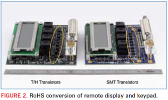
The savings achieved by the SMT migration completely offset the higher costs of Pb-free PCBs, components, and assembly. The net savings on the RoHS-compliant product was 2% per assembly. While this is not considered a substantial cost reduction, it is still far preferable to the anticipated cost increase.
Case 2: Analytical equipment controller boards. Before and after images of an industrial controller assembly are shown in Figure 3. This conversion required a replacement module with the exact same interface and functionality as the original to guarantee seamless integration into the final product. The BoM review indicated that the age of this product and its extensive use of PTH components offered multiple opportunities for cost reduction through redesign:
- Conversion of PTH to SMT components reduced main board area by 40%.
- Relocating opto-isolator to main PCB eliminated daughter card assembly.
- Reducing the component count and cost reduced the total BoM cost.
- PTH to SMT conversion reduced labor cost.
- Electrical redesign reduced cost of major components by using new, higher-capability processor chips. Logic and motor controls were consolidated into one processor, which also performed hardware control functions that were previously executed externally.

The reduction in PCB and manufacturing costs, and the benefits of component consolidation resulted in an overall savings of 31% per assembly.
Case 3: Real-time clock. The RoHS conversion of the real time clock and RAM backup module shown in Figure 4 was driven primarily by obsolescence. When faced with component obsolescence, the easiest option is often to purchase enough components to supply the product through the end of its lifecycle. In this case, however, the lifetime buy was not a viable option because the product had 10 years left in its lifecycle and required a five-year shelf life. The old modules were manufactured with internal batteries that would last at least five years but nowhere near 15 years.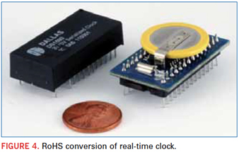
The new design had to address battery life issues and meet FDA requirements. Because the only alternative was complete redesign, RoHS compliance was added to its list of specifications. The redesign incorporated the following features:
- RoHS compliance.
- Battery installed at time of shipping final product, maximizing its shelf life and enabling easy replacement in the field.
- The exact form, fit and function of the new component exempted it from FDA recertification, saving the medical device manufacturer additional resources, time and money.
In addition to this redesign achieving RoHS compliance, extending the shelf life of the product and minimizing regulatory expenses, this conversion reduced the cost by a staggering 52% per assembly.
Case 4: Embedded process control board. Like Case 3, the conversion of the controller boards shown in Figure 5 was also driven by component obsolescence. These assemblies had two obsolete components, and more pending. One of the components was sourced through brokerage at 8X its original price! And like Case 2, extensive use of PTH technology made this a perfect candidate for redesign, even if the obsolescence issues were not considered.
Cost-reduction activities on this product included:
- Elimination of expensive, obsolete components.
- Consolidation of two PCBs into one using modern devices and fewer discrete parts.
- Addition of self-diagnostics to reduce test time by 66%.
- Fewer PTH components and more SMT components to improve manufacturing efficiency and reduce labor costs.
In addition to reducing cost, the redesign added functionality. It afforded the opportunity to incorporate new features requested by the customers, which included:
- Adding a USB port.
- Providing a more sophisticated communications protocol.
This conversion combined two PCBs into one, lowered the parts count, reduced test time and added functionality, while reducing product cost by 36% per assembly.
Strategies for Cost Reduction
Many factors influence the total cost of an electronic or electromechanical assembly, and most of them are interrelated. During the BoM scrub, the engineering team should look for opportunities to:
Reduce PCB size or count. PCB area and layer count are the biggest factors in PCB cost. Reducing area, which may be achieved by component count reduction or replacement of PTH with SMT components will reduce the PCB cost. Reducing layer count by using finer line spacing can also reduce PCB cost. And eliminating a PCB eliminates its cost completely.
Reduce parts count. Lowering the parts count usually lowers the total BoM cost. It can also shrink the PCB area requirement, improve manufacturing efficiency, and reduce labor/overhead/handling costs.
Reduce parts cost. Obsolete components are always more expensive than current ones, and mature, PTH components are almost always more expensive than modern SMT ones. Updating package types can save money; even older SMT packages often cost more than newer ones. Using up-to-date components that can combine multiple functions reduces parts cost, parts count, and PCB area requirements.
Convert PTH to SMT. As previously discussed, SMT parts are almost always less expensive than PTH parts; they require less PCB area, offer significantly better manufacturing efficiency, and reduce labor requirements.
Because the cost-drivers are so deeply interrelated, incremental design changes can generate substantial savings.
Discussion and Conclusion
While RoHS-compliant electronics products require more expensive PCBs, components and manufacturing processes, updating noncompliant products can actually save money. Electronics packaging and manufacturing technology progresses at such a rapid pace that updating the design of a legacy product using modern technology may reduce its cost, despite the typical price premiums associated with Pb-free soldering and other RoHS requirements. Many of the electronic assemblies facing the 2014 compliance deadline are excellent candidates for cost reduction due to their age and technology levels.
Four cases of RoHS conversion were presented, ranging from the simple BoM and footprint updates to complete redesign. Each project followed different conversion paths and employed different combinations of cost-reduction strategies, and all of them were more cost-efficient than their pre-RoHS ancestors.
The answer to the title question is yes, it is possible to reduce cost when converting electronic products to RoHS compliance. Overall cost-reduction depends on the age and technology level of the product. Keys to successful cost-reduction efforts include a thorough BoM scrub to help define the conversion path, a component consolidation strategy, incorporation of DfM recommendations, and consideration of testing requirements for validation and qualification.
Ed.: This article was originally presented at SMTA International in October 2012 and is published here with the permission of the authors.
Philip DiVita, David Steele and John Kanavel are with Da-Tech Corp. (da-tech.com); pdivita@da-tech.com. Chrys Shea is founder of Shea Engineering Services (sheaengineering.com); chrys@sheaengineering.com.
As manufacturers take care to wash traces of so-called Conflict Minerals out of their supply chains, many citizens of the Democratic Republic of Congo have been deprived the opportunity to live a better life by mining the precious ores beneath their feet. A small but growing group of major electronics OEMs and suppliers, together with the Dutch government, are working on a plan to ensure certain mines under the protection of the national army are certifiably “conflict-free.” One of those suppliers is Alpha. CIRCUITS ASSEMBLY editor in chief Mike Buetow spoke by phone with Alpha vice president of global marketing & corporate development Bruce Moloznik about the new initiative.
CA: What can you tell me about the Conflict-Free Tin Initiative?
BM: We are in fact part of that. We have been talking to people about the issue and going forward with what is hopefully a unified approach. In fact, we are involved in a lot of groups on the conflict minerals issue: the GeSI-EICC (auditor certification scheme), the CFS (The Conflict-Free Smelter Program), and the reporting template, where suppliers can identify where they get their tin. Let me clarify a few things about this, by the way. Conflict minerals are the minerals that tin, tantalum, tungsten and gold as a category are derived from. Conflict tin refers explicitly to tin from an illegal mine. The SEC rules cover any public company that uses tantalum, tin, tungsten or gold. The concern, and the reason this pilot is being put in place, is one thing: Will this work?
CA: How did Alpha get involved in the CFTI?
BM: We’ve been involved from early on in the pilot program, which was over a year ago. We drafted our policy and implemented it at the beginning of 2012. We strongly believe we have been offering conflict-free minerals since we became aware of the issue, but we ask all our suppliers to warrant they are not trading in conflict tin.
A lot of companies, in doing their audits, are looking at what their suppliers have done. The actual SEC SD (Supplier Declaration) is one page. If you find out your tin comes from the Congo, there’s a whole additional level of due diligence. The easiest thing for suppliers to do is to avoid it. But these minerals are the only assets the Congo has. The worst thing is the unintended consequence of a soft boycott on tin.
CA: When will the program begin?
BM: Our focus now is to get the first proof of concept through. There are many potential areas of cost increase involved throughout the supply chain. If all of the tin we needed to buy could be purchased conflict-free starting Jan. 1, this could be a smooth transition. But, I think this is going to be like lead-free, where companies will slowly transition and only then when forced to from the top of the supply chain. The addition, recycled material being allowed without the requirement of the original country mine of origin, was critical for the law to be implemented. This was based on the pervasive use of recycled material in our industry. The reporting period begins Jan. 1, 2013, and the only businesses that have to do this are US public companies, but, for example, for Asian companies that sell to public companies, the US company’s due diligence will rely on their supplier’s due diligence, who actually purchases the tin-containing material.
If yours is a smaller US company, and none of your goods are sold into public companies, you won’t be affected. There are certain European companies that will piggyback on this law. Europe won’t be insulated, but it will be voluntary. By the end of 2013, these companies will have to put together all this due diligence to prove what they did to keep conflict tin from their supply chain. Not all smelters will be certified as of Jan. 1, and some may never get certified.
CA: How is mine security handled for the pilot?
BM: The smelter is the supplier that buys directly from the mines and is transparent about having bought from the DRC. This partner smelter is in the process of getting their Conflict Free Smelter certification. ITRI is a key player in putting this pilot together on the ground. They are involved with others in the “bagging and tagging” cassiterite with a seal that indicates the Source Mine of the material is a conflict-free mine. That bag’s contents will be transferred to a consolidator and sold to the smelter and smelted with other conflict-free tin. Alpha will buy this certified conflict-free tin, and we will not cross-contaminate it with other mainstream sources – to make conflict-free finished goods.
CA: Does it make economic sense today to buy conflict minerals?
BM: It is unclear what will happen to price. When you buy metals, you buy at the LME (price), plus traders’ fees, shipping and freight. We’re going to have to demonstrate the value customers are getting. Even if every smelter in the world could suddenly on Jan. 1 provide conflict-free tin, Alpha will still need new labels, new traceability IT systems, and have other costs that will increase our cost base in an already extremely price competitive environment.

Press Releases
- RBB Welcomes Shawn Myers as Engineering Project Manager
- ECIA’s Market Sentiment Index Average Hits Five-Year High in June Industry Pulse Survey
- Incap Slovakia invests in cleanroom capability to support semiconductor manufacturing requirements
- Orbit Technologies accelerates growth and doubles production capacity with Europlacer iineo placement machine