

Results of a study comparing traditional rework methods to a novel stencil process.
Recently, the impact of leadless device reliability after rework was investigated as part of a NASA/DoD project for different leadless device rework processes. Leadless device packages, which are challenging to rework due to their large thermal ground planes, low standoff heights from the PCB and the lack of visually inspected criteria, were investigated for their long-term reliability after rework. Several leadless device rework methods, including the latest rework procedure (stay-in-place stencil)1, were investigated in this study. The study, commissioned by Naval Surface Warfare Center (NSWC), Crane Division was attempting to answer: To what extent do rework procedures, including SnPb and Pb-free mixed solder joints, affect solder joint reliability of high-performance electronics?
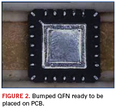
Numerous methods are used to rework leadless devices, either guided by the older IPC-7711, Method 5.4.1 process guidelines or the newest stenciling techniques. The older of these methods includes solder paste printing the site location on the PCB, followed by placement and reflow of the device. The newer method includes the device pad “bumping,” followed by placement of the device with a rework system using paste flux (Figure 1).
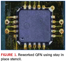
Several years ago, a simpler, faster method for reworking leadless devices was developed using polyimide stencils. In this method, a polyimide stencil is placed over the land patterns on the bottom of the device. Solder paste is then rolled into the apertures. After reflow, the stencil is peeled off, leaving “bumps” on the bottom of the device (Figure 2). A stencil permanently affixed to the PCB filled with paste flux or solder paste then acts as the receptacle for these device “bumps” to fit in to. However, heretofore the longevity of such an interconnection was questioned. This study, a portion of which is described in this writing, verifies the reliability of these solder joints using this newer technique.
Method
The goal of the NASA/DoD project was to generate data supporting qualification of SnPb rework procedures for military hardware built with Pb-free processes through analysis of thermal cycling, vibration and drop test data, including micro-section analysis.
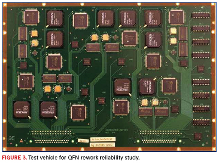
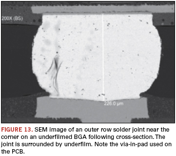
Thirty of the 193 test vehicles were built for Crane, in support of the larger Naval Supply Command (NAVSUP)-sponsored Logistics Impact of Pb-free Circuits/Components project. PCBs were assembled using SAC 305 Pb-free solder alloys using boards with Pb-free component finishes. The boards had an FR-4 laminate per IPC-4101/26 with a minimum glass transition (Tg) of 170ºC for the test vehicles. Bare boards complied with IPC-6012, Qualification and Performance Specification for Rigid Printed Boards, Class 3, Type 3 specifications. The boards had an immersion silver finish and were processed per IPC-4553, Specification for Immersion Silver Plating for Printed Boards. The test vehicle was 14.5"x 9" x 0.09" with six 0.5-oz. copper layers (Figure 3).
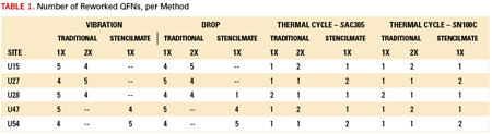
Following assembly, rework was performed on random Pb-free DIP, TQFP-144, TSOP-50, MLF, LCC and the QFN components of interest using SnPb solder. Components were reworked either once or twice. QFNs were reworked using two methods. In the first method, boards were PCB device locations paste-printed on the boards using rework systems. Devices were removed per IPC-7711, Method 3.11. In the second method, parts were bumped IPC-7711, method 5.8.1.2. Once bumped, the parts were inserted into the stencil on the board. The matrix of the experiment is in Table 1.
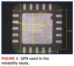
The particular focus of this paper is related to the QFN package (A-MLF20-5mm-.65mm-DC) as seen in Figure 4. The test plan was chosen to represent performance requirements in applicable military and industry standards. A key factor was selecting test parameters that would subject enough environmental stress to cause solder joints to fail, thus permitting differentiation between lead vs. Pb-free performance. MIL-STD-810F, IPC-SM-785 and IPC-TM-650 were primary references used for writing the test plan.
Numerous tests were part of the overall test protocol. The vibration test was instituted per MIL-STD-810F, Method 514.5 (Vibration), to determine reliability of the various solder alloys under severe vibration. Thermal cycle testing used was performed in accordance with IPC-SM-785, Guidelines for Accelerated Reliability Testing of Surface Mount Solder Attachments, to determine the longevity of the solder joints under thermal stress conditions. It was conducted at two different conditions: -55° to +125°C and -20° to +80°C. Thermal cycle tests were run until greater than 63% of component failures were achieved in order to provide statistically meaningful data. The mechanical shock test was used to determine solder resistance to the stresses associated with high-intensity shocks induced by rough handling, transportation, or field operation. The Combined Environments Test (CET) was used to predict reliability of solders under combined thermal cycle and vibration. Finally, drop testing was used to determine resistance of board-level interconnects to board strain induced by dynamic bending. These failure modes replicate the stresses seen during manufacturing, electrical testing (especially in-circuit test), card and field installation due to process issues and/or the quality of incoming components and/or boards.
Results
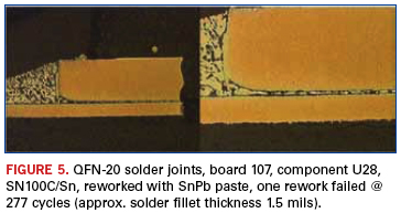
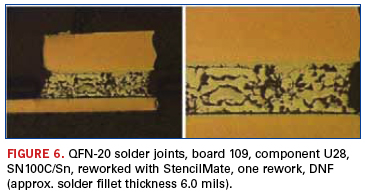
The polyimide stencil reworked solder joints were significantly thicker than the traditionally reworked solder joints (Figures 5 and 6).
Thermal cycle testing. Thermal cycling testing was conducted between -55° and 125°C per http://teerm.nasa/gov for NASA-DOD Lead-Free Electronics. The temperature was cycled between -55° and 125°C at a maximum rate of 10°C/min and a dwell time of 30 min. at 125°C and 10 min at -55°C. A total of 4,068 cycles were completed. Electrical continuity was continuously tested, and failure was recorded corresponding to the total number of cycles.
Vibration. Vibration testing was conducted per the study’s test protocol (available at teerm.nasa.gov). Test vehicles were evaluated at eight intensity levels from 8 to 28G. Each intensity level was evaluated consecutively, starting with 8G and increasing in intensity every 60 min. Table 3 outlines the vibration profile for each level as programmed for the shaker table. For all levels, the power spectral density (PSD) increased at the rate of 6db/octave between 20 and 50Hz and decreased at the rate of 6dB/octave between 1000 and 2000Hz.
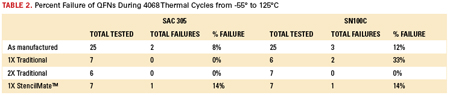
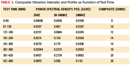
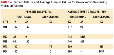
Table 4 shows results from the comparison of percent failure and time to failure for reworked QFNs. Percent failure was calculated by dividing the number of components in a group that failed during testing by the total number of components in that group. Average time to failure was calculated considering components that did and did not fail during testing. Differences in time to failure are considered significant if the percent failure differs by at least 40%. Drop shock, as well as other reliability test results, can be found on the teerm.nasa.gov website.
Conclusion
Based on the extensive reliability testing undertaken in this study, it was determined that independent of the QFN rework method, the polyimide stay-in-place stencil technique performed at the same level as traditional board paste printing. Based on thermal shock and vibration testing (as well as shock, combined environmental and drop testing), there was no difference between rework methods. These results have shown that this simple-to-implement technique has been shown to not impact the reliability of a reworked device. In fact, the microsections indicate that the stay-in-place polymide stencil technique, if time allowed, would outlast traditional hot air rework methods.
Bob Wetterman is president of BEST Inc. (solder.net); bwet@solder.net.
References
1. IPC-7711/IPC-7721B, Rework of Electronic Assemblies, 2008.
2. J.P. Tucker, C.A. Handwerker, A.E. Pedigo, et al, “NASA-DoD Pb-Free Electronics Rework Project: Effect of 1x and 2x Eutectic Solder Rework on Vibration Reliability,” SMTA International Proceedings, October 2011.
3. National Aeronautics and Space Administration, “NASA-DoD Lead-Free Electronics Project,” March 2010.
4. NASA-DoD Lead-Free Electronics Project Joint Test Report - Final, “Technology Evaluation for Environmental Risk,” December 2011.
5. National Aeronautics and Space Administration, “NASA-DoD Lead-Free Electronics Project,” September 2009.
6. Daniel Staubach, “QFN Rework in OEM Quality,” EMT Worldwide, March 18, 2008.
Perfect thermocouple placement is necessary for optimized profiles.
Growing numbers of printed circuit boards are now denser and smaller to comply with wireless and portable applications, bringing a new round of challenges to create the proper thermal profiles. Even the smallest boards come in a vast number of sizes, shapes and thicknesses, and each requires a unique thermal profile for a perfect assembly process.
No two boards are alike. Consequently, it is of utmost importance to develop a one-of-a-kind thermal profile for each board. Size matters: Smaller PCBs subjected to reflow withstand a lower duration peak temperature cycle than do larger ones. And some boards are more populated with components than others. With compact designs growing in popularity, most PCBs have both sides populated with ball grid arrays (BGA), µBGAs, chip-scale packages (CSP), µCSPs, quad-flat no-lead packages (QFN), dual-flat no-lead packages (DFN), and other devices.
Thermal profiles take into account the size of the PCB and the number of critical components to be installed, along with several other factors. Profiles for SnPb and Pb-free are different because Pb-free solder requires a higher peak temperature. Each board side requires a unique profile. The thermal profile for the bottom side is developed first. The reasoning is this: When the bottom side is profiled and undergoes reflow, less heat is applied to the topside of the board since it is not yet populated. When the topside is profiled and the bottom side is already profiled, more heat is required so that components on the topside are properly reflowed and to make certain that the desired soldering temperature is achieved for that side of the board.
Thermocouples in the right place. Small PCBs might be processed in panels. Because the boards are smaller, the boards are presented in array form so they can be run through the SMT assembly line more efficiently. The number of boards per panel can vary. [Ed.: For more on arrays, see “The PCB Array, and Why We Use It,” PCD&F, June 2012.] Creating a profile for a specific small board can be tricky because thermocouples need to be placed on the boards in a number of distinct and correct ways.
For larger boards, placing thermocouples at the right place isn’t such a problem because a baseline profile is needed for any size board. This profile is the startup profile for a given assembly. This profile might be defined based on the process engineer’s experience.
For boards in array or panel form, however, thermocouples are placed in the areas where critical components are located (Figure 1). These components are BGAs, QFNs, DFNs, CSPs or any other temperature-sensitive components that cannot withhold temperature above certain threshold limits, based on manufacturer’s specification defined in a datasheet. Figure 3 shows thermocouple (TC) placements on different boards. The TCs are placed on the PCB where a dummy component is placed before sending the board through the oven. Data are gathered and a profile generated after the board comes out of the oven. The profile is then evaluated and adjusted as needed.

Sometimes, certain components require special attention during reflow due to temperature requirements, as well as limitations for a particular device or component. Some parts cannot exceed a specific temperature range. In particular, µBGAs and µCSPs require lower temperatures compared to larger packages because of their lack of size. The number of balls on the µBGAs and µCSPs is fewer; therefore, less heat is necessary to establish a good profile.
As for thermocouple placement, if a particular PCB has, for example, two BGAs in the board and comes in a panel of four small boards, thermocouples need to be placed in those eight locations of those four boards. Optionally, thermocouples could be placed in strategic areas where thermal readings are critical. For the most part, these areas are where BGAs, CSPs, QFNs and other critical devices are located.
Thermocouples provide the actual temperature reading from the specific areas where they are placed on the PCB. These readings indicate if the reflow profile is optimized or in need of adjustments. Figure 2 shows the actual peak temperature of U1 at 241.51ºC. This profile is for a Pb-free assembly, and the manufacturer’s suggested peak temperature range is between 230ºC and 250ºC. With a little bit of a tweak of the temperature settings on Zones 2, 3, 6 and 8, the predicted peak temperature is now at 244.28ºC. Different contract manufacturers have different requirements when generating reflow profiles for each assembly. Experience and the solder paste manufacturer’s reflow profile guidelines play a big role.

Thermocouples on micro devices. Thermocouples are placed on such devices as µBGAs and µCSPs to achieve the optimum profile for that given board and to ensure proper wetting occurs. The goal is not to overheat these parts or the PCB, lest they be damaged from the excessive temperature. By getting the most accurate readings on the areas where the critical components are placed, avoid overheating and damaging them.
PCBs measuring 2" x 2" or less are particularly challenging when it comes to thermocouple placement. If that board has more than three areas requiring temperature readings for a correct profile, there is no space on that small board to place three or more thermocouples. That particular PCB has to undergo reflow at least twice to get an optimized profile.
This challenge becomes compounded if the customer doesn’t provide a solder sample. As a result, the process engineer has to use a good board to develop the profile. That particular board is run through reflow once, rather than running a solder sample board multiple times inside the reflow oven. Getting a solder sample from the customer is a key item when preparing a reflow profile on any given board.
It is particularly important to strategically place thermocouples on µBGAs and other smaller packaged devices to get accurate temperature readings (Figure 3). The temperature reading plays an important role for thermal profile development. These readings tell the process engineer if his or her profile needs adjustment or not. Temperature readings are compared to the solder paste manufacturer’s recommended application reading and reflow guidelines. The target is to get as close to the manufacturer’s reflow guidelines as possible, in order to have a 100% accurate board assembly.

By placing thermocouples on those components, data are collected to determine if certain areas are being overheated or whether some areas aren’t getting enough heat. Therefore, some adjustments are needed on the temperature settings. Applying too much heat causes component failure or causes flux to evaporate from the solder paste, making the assembly more prone to brittle joints that can create a latent defect in the field.
Also, if no temperature readings are taken on these critical components, the profile will not be optimized for a particular board. Various process issues may occur, resulting in unnecessary rework and project delays. For instance, a voiding – where a BGA is not 100% collapsed and a gap exists between the BGA and PCB – is one of the more common defects. The reason could be a lack of uniform localized heating on the BGA balls.
Another consideration when deciding where to place thermocouples on a particular panelized board is the component placement. If components are located on the edge or middle of a large conventional board, thermocouples are placed in those areas to obtain actual temperature readings and adjust accordingly. On a small, panelized board, the thermocouples are still placed at locations where critical components are placed. Subsequently, thermocouple placement is evenly distributed on the panelized PCBs to be manufactured.
If placement is incorrect, an inaccurate thermal profile results. Temperature readings will be imprecise, and the reflow profile will need to be revisited. Process issues, such as voids, shorts or cold solder, will occur if thermocouples are randomly placed on a board without considering proper placement. If erroneously placed, the benefits of efficient temperature readings are lost, and the board could be damaged during reflow.
With excessive heat come possible delamination issues on the PCBs where the board reliability is compromised. For small boards, in particular, delaminating is a problem that can arise by not creating the right thermal profile. If temperature settings are too high, “bubbling” on the board can occur (Figure 4). Bubbling is a form of delamination that causes the top layer of the PCB to rise up like a bubble and creates reliability issues. Various areas on the board can delaminate, which decreases the integrity of the PCB. Damaging costly components on the board is another problem. Tombstoning is yet another issue that can arise when too much heat is applied to the board. This is where one side of the component is pulled, causing the other end to stand up.

It’s worth noting there are sensitive components that cannot handle high temperatures and may fail during testing. They are regarded as sensitive based on their susceptibility to heat. Some devices like a µBGA, for example, cannot be exposed to temperature exceeding 230°C. Thermocouples are placed on the areas where these components are located on the board. Once data are collected, the profile is evaluated and temperature settings adjusted accordingly until an optimum reflow profile is achieved.
Simon Ilustre is a process engineer at NexLogic Technologies (nexlogic.com); info@nexlogic.com.
As China matures, a host of factors could rebalance the geographical supply chain.
Nearshoring and reshoring are significant topics of discussion in the outsourcing community. Factors that led China to become the world’s workshop are shifting. China’s labor costs have doubled in the past two years and will likely grow another 15% to 20% in 2012. Some OEMs are simply looking to move business to other countries in Asia. Fuel costs and recent natural disasters are key reasons why many are looking closer to home to lower their risk with shorter supply chains. Tighter credit is making inventory buffers more expensive to maintain. All this has led Boston Consulting Group to predict that by 2015 the percentage cost differential between China and some parts of the US will be in the single digits.1
As few as five years ago, those without an “Asia plan” risked being left behind. Today, OEMs that lack a nearshoring strategy are the ones that risk falling behind. At Spectrum Assembly, we see many companies starting to evaluate the true cost of nearshoring vs. offshoring, particularly with high-mix projects. A Pennsylvania State University study found that most companies took a fairly unsophisticated approach to analyzing offshore sourcing costs.2 The key is balancing tangible landed cost against risk factors that are hard to put into dollar amounts. We see several cost and risk factors routinely overlooked in initial cost evaluations. What are the potential cost impacts to evaluate in each of these areas?
Regulatory supply base constraints. Products in highly regulated industries may have very limited supply base options relative to certain components. For example, one of our customers whose products were used in the nuclear industry could use only raw cable that met very rigid industry specifications. The only two suppliers of that type of raw cable were located in the US. An offshore build required shipping raw cable to China, assembling the product and then shipping it back to the US. Add air freight costs to support demand variations of a build-to-order product, and a US build was clearly the most cost-effective option.
Intellectual property theft risk. IP theft is always a risk in certain geographies. Variations in IP laws between countries can make IP violations expensive to prevent. Litigation is expensive wherever you are. Lost market share can be difficult to regain. For products that will be sold in the countries in which they are manufactured, this is simply a cost of doing business. However, if the product will not be sold in that region, the costs of maintaining IP protection in that region should be evaluated.
OEM team time and travel costs. Fit between teams is an important part of a successful outsourcing relationship. The level of product maturity and project complexity dictate how much time sourcing, engineering and contractor teams need to spend together. The cost of deploying teams at a distance, extended work hours to support multiple time zone teleconferences and potential language or communications issues should be considered in a total cost evaluation. Another driver is preference for the convenience of a local supplier when significant engineering interface is required.
Quality concerns. Most OEMs audit to ensure an offshore contractor has acceptable levels of quality. Contractors in these regions are used to substituting wherever they can to reduce cost or keep lines running, and on-the-fly AVL changes are common. If the contractor isn’t watched, unauthorized substitutions may be inadvertently made. This can create significant issues for companies in regulated industries such as medical equipment or in any mission-critical product that requires third-party design approval or registration. Quality issues can creep in over time, particularly in high-mix projects. As a labor market matures, personnel turnover increases. This in turn drives learning curve quality issues as replacement personnel are hired and trained. A factory in China can experience turnover of upwards of 80% season to season. The standard training strategy with a high turnover workforce is to train them well on a specific task with few product options. Comparatively, onshore companies focus on developing low turnover workforces through pay-for-skills programs, and lower labor costs by using fewer employees to perform a wider variety of tasks. As an example, over 50% of our production operators have been with Spectrum Assembly more than a decade.
Alignment with contractor’s business model. Two dynamics are changing the model in Asia. First, internal demand is causing China to go up market. Simple jobs are being no bid in favor of more challenging work with more value-add. Second, the recent disasters in Japan and Thailand drove offshore contractors to implement disaster recovery plans and prioritize work for their most important customers. The OEMs whose production was delayed in favor of contractors’ larger customers are now looking for partnerships with contractors who see them as a fundamental part of their business strategy.
Expedited shipping costs driven by demand variations. Another challenge is that demand is hard to forecast. Most top distributors will say that in North America the mean average deviation (MAD) on a 30-day horizon is not much better than 50%. As a result, OEMs with higher mix product lines have greater schedule flexibility if they assemble locally with an onshore contractor and a Lean supply base philosophy where variations can be addressed fairly easily. With an offshore pipeline, variations may trigger air freighted shipments. One or two overseas premium air shipments can completely cancel out any labor savings.
Resource opportunity costs. The first benefit that most OEMs look for to justify an outsourcing project is the variable cost savings embodied in landed price. When offshore and onshore pricing is near parity, resource opportunity costs need to be carefully analyzed. For example, longer pipelines driven by sea shipments increase the potential inability to meet varying customer demand. Onshore suppliers reduce or eliminate team travel time and usually require less oversight than offshore suppliers. Time zones are more compatible to normal working hours. In short, there is a significant savings related to non-value-added time spent on the project when a domestic partner is used. Eliminating that non-value-added time frees those resources. From an inventory perspective, working capital is reduced or can be redeployed in ways that increase a company’s ability to respond to variable demand. From a personnel standpoint, team members can be redeployed to next-generation product development or launching entirely new product lines.
Nearshoring is not right for every product. However, focusing on these cost drivers can help identify products that would benefit from this strategy. All labor markets eventually mature and increase in cost. A strong offshore/nearshore total cost analysis process is critical in ensuring that sourcing teams make the most cost-effective decisions.
References
1. H. L. Sirkin, M. Zinser and D. Hohner, “Made in America, Again. Why Manufacturing Will Return to the US,” Boston Consulting Group, August 2011, p. 3.
2. R. Young, P. Swan, E. Thomchick and K. Ruamsook, “Extending Landed Cost Models To Improve Offshore Sourcing Decisions,” International Journal of Physical Distribution & Logistics Management, vol. 39, no. 4, 2009 p. 320.
Wally Johnson is vice president, sales and marketing, at Spectrum Assembly Inc. (saicorp.com); wally@saicorp.com.
Underfilms have material properties similar to underfills but are easier to process.
A common failure mode for portable electronics is mechanical failure as a result of being dropped from sufficient height to cause damage. Most portable electronics producers qualify assemblies by performing some type of system-level drop test, while component suppliers typically utilize industry standard drop tests such as JEDEC JESD22-B111.1 It is well known that Pb-free solders do not perform as well in drop or shock testing as the Pb-free solders they replaced.
Much work has been carried out to optimize Pb-free alloys to improve drop test performance.2-6 Many companies have also implemented epoxy underfill to further increase robustness of the interconnection between the BGA and printed circuit board. These underfills are typically dispensed around the BGA following SMT assembly and electrical testing. Capillary action then slowly draws the underfill under the BGA. The underfill may be dispensed in sufficient volume to cover the entire BGA underside, the corner areas only or just the package sides. Finally, the underfill is cured in an offline batch oven. While excellent drop test results have been demonstrated with underfill, the process adds cycle time and may involve processes not normally performed during assembly. Another option for providing greater BGA to PCB mechanical robustness that may provide a more seamless integration into the SMT manufacturing process is the use of a preform underfilm material.7 The material can typically be provided in reels similar to discretes and is placed around the perimeter of the BGA following solder paste printing and prior to BGA placement. In reflow, the underfilm softens and initially expands such that it contacts both the BGA and the PCB. By the conclusion of reflow, the material fully cures, while remaining adhered to both the BGA and PCB.
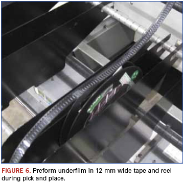
For our study, the preform underfilm material was a fully cured, low flow polyurethane polymer. It comes in a variety of shapes and sizes, and for this study it was specified in 4.0 x 0.76mm preforms with a thickness of 0.165mm. The preforms were provided in EIA-481-compatible 12mm wide carrier tape with a cover tape similar to how discretes would be supplied. The underfilm material is a thermoplastic designed to soften, flow and expand during reflow, thereby filling in the gap between package and PCB. Upon cooling in the reflow oven, the material resolidifies and bonds the package to the PCB. For this study, it was decided to use two of the preforms per corner, which effectively formed an L-shaped pattern. It should be noted that L-shaped preforms could also have been used.
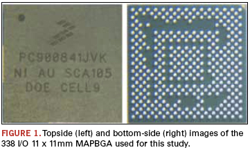
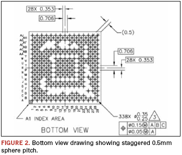
The test vehicle (Figure 1) was a 338 sphere 11 x 11mm body size PBGA with spheres at a staggered 0.5mm pitch (Figure 2). It is a package typical of portable electronics applications. The composition of the Pb-free spheres was SAC 105 (98.5%Sn, 1.0%Ag, 0.5%Cu by weight). The PBGA was molded all the way to the substrate edge in what is called a Mold Array Process (MAP).
The dummy die size inside the daisy-chain package was 5.3 x 5.4 x 0.28mm; the two-layer substrate thickness was 0.21mm, and the total package thickness excluding spheres was 0.92mm. The pads on the package were SMD with a specified 0.38mm copper diameter and a 0.30mm soldermask opening.
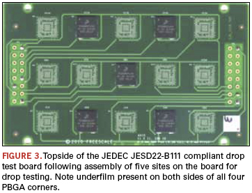
The test board used was based on the JEDEC drop testing specification for devices with less than or equal to a 15 x 15mm body size. The board (Figure 3) was 132 x 77mm and 1.0mm thick with eight layers of copper. The surface finish was OSP. SMD pads on the PCB were designed to exactly match the package, with a copper diameter of 0.38mm and a soldermask diameter of 0.30mm. The only modification made to the test board to accommodate the underfilm preforms was the addition of four additional pads in each corner of the package footprint. Once printed with solder paste, these tacky pads served as a way to keep the underfilm in place prior to reflow.
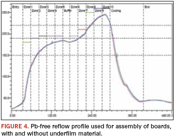
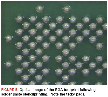
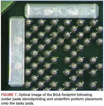
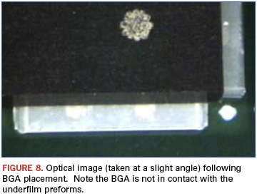
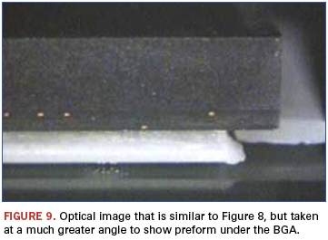
Assembly was carried out using a high-volume production SMT line with automated pick-and-place equipment and automated solder paste volume inspection. PBGAs were supplied in JEDEC trays. The Pb-free solder paste used was a halogen-free, no-clean with a SAC 305 composition (96.5%Sn, 3.0%Ag, 0.5%Cu). The reflow profile (Figure 4) had a peak temperature of 244.5º to 246ºC, depending on thermocouple location. Total reflow time was approximately six minutes. Each underfilm preform was placed on the two tacky pads near each corner of the part following solder paste printing. BGAs were then placed normally. Figures 5 to 10 show photos taken at various steps in the assembly process from printing and underfilm preform placement through BGA placement and reflow.
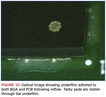
As shown in Table 1, a total of 14 boards containing 130 total components were assembled. On the boards for drop test, only five sites were populated (Figure 3). This is permitted by the JEDEC standard and was done to provide the most consistent drop test results by not populating parts close to corner standoffs. For the boards for thermal cycling, all 15 sites were assembled. Two additional boards were assembled for cross-sectioning. One hundred percent yield was achieved in assembly, and all underfilmed BGAs appeared to have the material adhered as expected between the BGA and the PCB in all four corners.
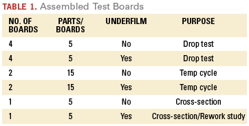
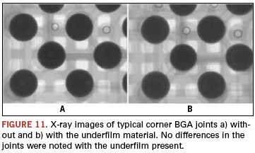
X-ray analysis. Following assembly, all boards underwent x-ray, with close attention paid to corner joints that may be in contact with the underfilm material. No misshapen or anomalous solder joints, such as those with opens, shorts, or excessive voiding, were observed (Figure 11). Additionally, the tacky pad locations were x-rayed, and all the printed solder paste was seen to be soldered to the pad, as opposed to being dispersed in the underfilm (Figure 12).
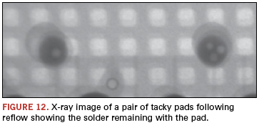
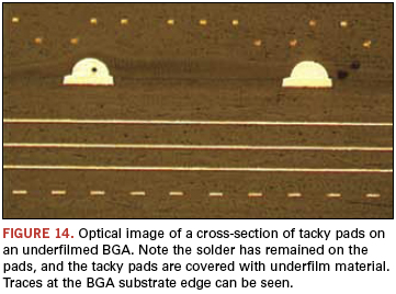
Cross-sectional analysis. Underfilmed and non-underfilmed BGAs were both cross-sectioned to the outer row to assess the solder joint formation and standoff (Figure 13). The underfilm was seen to be enveloping the three to four solder joints closest to the corner. The solder joint standoff between the underfilmed and non-underfilmed BGAs was found to be similar. A cross-section through the tacky pads on an underfilmed sample further confirmed that the solder paste reflowed and remained on the tacky pads (Figure 14).
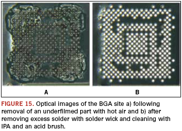
Underfilm rework evaluation. Using an extra board that was assembled with underfilm, a small study was carried out to ascertain the reworkability of underfilmed BGAs. Since the material softens at elevated temperatures, parts were removed using a hot air rework station using a standard rework cycle. A slight upward force was used to remove the BGAs once the Pb-free solder spheres melted. Excess solder was then wicked from the BGA pads and the entire area cleaned up with IPA and an acid brush. The resulting sites appeared to be underfilm-free and ready to accept another BGA (Figure 15).
Board-level thermal cycling. Boards populated with 15 parts per board were placed into thermal cycling, for a sample size of 30 parts with underfilm and 30 control parts without. The single chamber cycle went from 0º to 100ºC with 10 min. ramps and dwells for a cycle time of 40 min. or 36 cycles per day. As of this writing, the boards had gone 3,000 cycles with no failures in either group. This would far exceed most requirements for handheld portable electronics.
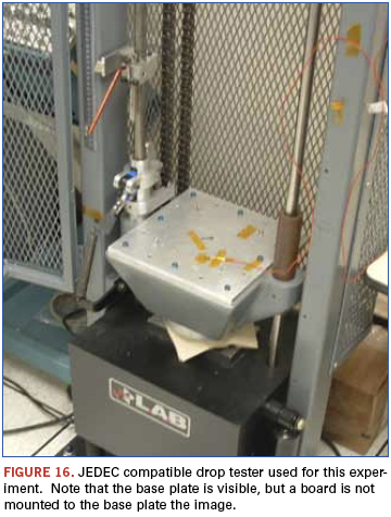
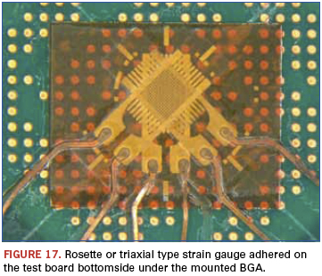
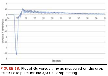
JEDEC drop testing. Drop testing was carried out using a JEDEC-compatible drop tester (Figure 16). During the drop, continuity to the daisy-chain parts was continually measured using a high-speed event detector. Additionally, triaxial strain gauges were affixed to the PCB on the bottomside of the BGA footprint to measure strain during the drop (Figure 17). Boards were attached to the base plate on the drop tester using four steel standoffs in the board corners. The JEDEC standard calls for boards to be dropped to Condition B, which is 1,500 Gs, as measured on the base plate with a 0.5ms duration and half-sine pulse.
Two of the underfilmed boards and two of the non-underfilmed boards populated with five parts each were initially dropped 100 times at 1,500 Gs. No electrical failures were recorded on any of the four boards. It was decided to drop the remaining four boards to the maximum 120cm height on the drop tester to achieve failures in a reasonable amount of drops to enable assessment of the performance of the underfilm material. Dropping from this maximum height resulted in approximately 3,500 Gs being recorded on the accelerometer on the base plate. See Figure 18 for a typical accelerometer output during a 3,500 G drop. The 3,500 G drop also resulted in a maximum of approximately 1,500µm strain being recorded on the strain gauge under the mounted BGA. One non-underfilmed board was dropped 118 times and the other 140 times, resulting in four of the five parts failing on each board. The first of these failures was recorded at 20 drops. The number of 3,500 G drops to failure for these two non-underfilmed boards is plotted on Weibull axes (Figure 19).
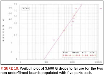
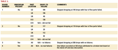
One underfilmed board was then dropped 300 times at 3,500 Gs with no failures recorded on any of the five parts. The intention was to drop the other underfilmed board 300 times, but following 163 drops, a failure was recorded on one of the underfilmed BGAs. The test board was inspected and was found to have broken in the corner where it attached to a standoff. The part that recorded the failure was located in the broken corner. This failure was discounted, and drop testing was terminated at this point. If a true failure had occurred on this board at this point, the underfilm material would have increased the drops to first failure by at least eight times (20 versus 160+ drops) versus non-underfilmed parts. If this second board had not experienced a PCB fracture and experienced no failures out to 300 drops as the other underfilmed board did, the underfilm material would have provided a 15 times improvement in drops to first failure. All 3,500 G drop test results are summarized in Table 2.
Drop testing failure analysis. A non-underfilmed part that had a failure at 104 drops was subjected to dye penetrant analysis following 140 drops.8 Typical solder joint fracturing was observed in the BGA corner (Figure 20). Since no true failures were recorded on any underfilmed parts, no analysis was performed on these.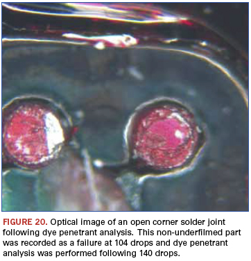
Conclusions
A preform underfilm material designed to be a drop-in to the SMT process was evaluated for assembly characteristics, yield, drop test performance and thermal cycling reliability. The following conclusions were drawn from the study:
- The preform underfilm material was seen to be a drop-in to a conventional, high-volume SMT process and was handled and pick-and-placed very similar to discretes.
- Only a small design change was carried to the test PCB to accommodate the underfilm material. Tacky pads were added to the footprint to prevent any movement of the preforms prior to reflow.
- One hundred percent SMT assembly yield was achieved with 21,970 0.5mm pitch joints formed robustly on 65 BGAs containing the underfilm material. Following reflow, all BGAs with underfilm appeared to have the material adhered as expected between the BGA and the PCB in all four corners.
- The underfilm material had no observable effect on solder joint shape or standoff on the corner joints it came in contact with.
- Using a JEDEC-based drop test at a severe 3,500 Gs, drops to first failure was increased by a minimum of eight times and probably much greater (15 times or more) with the use of the underfilm material. An exact improvement factor could not be determined since no actual drop test failures were recorded with the underfilm material.
- Initial results suggest the underfilm material results in no degradation in thermal cycling performance. Thermal cycling to at least 50% failure continues.
Acknowledgments
The authors wish to acknowledge David Mendez and Kirk Kringel at Flextronics for technical and logistical assistance, Randy Temple and Dave Skupien at Alltemated for supplying the underfilm material along with applications assistance, Terry Burnette at Freescale for carrying out the rework evaluation, Scott Stoller at Freescale for performing the drop testing, Roy Arldt at Freescale for cross-sectional analysis and Ed Hall at Freescale for management support of this project.
References
1. JEDEC JEDS22-B111, “Board Level Drop Test Method of Components for Handheld Electronic Products”, July 2003, www.jedec.org.
2. C. Chiu, K. Zeng, R. Stierman, D. Edwards, and K.Ano, “Effect of Thermal Aging on Board Level Drop Reliability for Pb-free BGA Packages”, ECTC, p.1256, June, 2004.
3. D. Henderson, “On the question of SAC solder alloy – Cu pad solder joint fragility”, Webcast Meeting on SAC Solder Joint Fragility, Binghamton, NY, September, 2004.
4. S. K. Saha, S. Mathew and S. Canumalla, “Effect of Intermetallic Phases on Performance in a Mechanical Drop Environment: 96.5Sn3.5Ag Solder on Cu and Ni/Au Pad Finishes”, ECTC, S29p5, June, 2004.
5. M. Amagai, Y. Toyoda, T. Ohnishi, S. Akita, “High Drop Test Reliability: Lead-free Solders”, ECTC, S29p7, June 2004.
6. Alltemated Place-N-Bond Pick-and-Place Underfilm product data sheet, http://www.alltemated.com/img/Place-N-Bond-Underfilm-data-sheet.pdf?vsid=ypxrplzu.
7. W. Liu and N.-C. Lee, “Novel SACX Solders with Superior Drop Test Performance,” Proceedings of 2006 SMTA International, September 2006.
8. T. Burnette and T. Koschmieder, “Solder-Joint Failure Analysis”, Advanced Packaging, January 2003, pp. 25-27.
Ed: This article was first published at SMTA International in October 2011 and is reprinted here with permission of the authors.
The authors are with Freescale Semiconductor (freescale.com); andrew.mawer@freescale.com.
Mid-market providers are responding to OEM desires for more regional approach.
As wages continue to rise in China and fuel costs escalate worldwide, some North American manufacturers are reevaluating their global operations to determine if production locations are optimal. This is reinvigorating discussion among EMS providers over whether China or Mexico is the best site for lower-cost production.
Both locations have inherent pros and cons, but unlike a decade ago when the World Trade Organization welcomed China as a new member, a comparison of China with Mexico can no longer be based solely on input costs, i.e., labor and transportation. Global electronics supply chains have evolved to be much more complex, and OEMs are demanding faster and more solutions-focused services from EMS suppliers. At the same time, the economies of North America and Asia have changed dramatically since 2000, with growth slowing in the West just as thousands of poor Chinese people are joining the middle class.
The decision for EMS providers, then, turns on cost strategy and customers; the best location, under the best circumstances, is the one that satisfies both.
According to Sonny Newman, president of Reno, NV-based Electronic Evolution Technologies (EE Tech), the EMS company’s Empalme, Sonora Region, Mexico, location gives it a unique strategic advantage over competitors without a Mexico manufacturing location.
“The strategic advantage that our customers enjoy with us in Empalme versus Reno is a lower labor and overhead cost out of our Mexican production facility,” Newman says. “By taking a few more weeks to have the product built in Empalme versus Reno, a customer can save a substantial amount. Unfortunately, the material cost is the same, and that represents a large percentage of the builds, but when you are producing thousands or even hundreds of thousands of units, that savings adds up very quickly.”
To deliver this savings advantage, EE Tech works collaboratively with The Offshore Group to run its Mexico operations. The Offshore Group is what is known in Mexico as a “shelter,” or outsourced manufacturing support company.
“The strategic advantage that we have operating in Mexico is made possible by our partnership with The Offshore Group. They handle the functions of our operations that, although not related to actual manufacturing, are critical to our being able to be and remain up and running profitably. Because they handle things like managing our payroll and worker benefits, our import and export operations and worker transportation, as well as maintaining our manufacturing facility, we can focus on our manufacturing mission, which is where we add lasting value for customers.”
Doug Besse, executive vice president, global supply chain and Asian operation manager for Creation Technologies, a global EMS provider based in Canada, also says his company takes a customer-centric approach to making plant-location decisions.
“Creation Technologies looks at it and says that we really need a Mexican manufacturing location for different reasons than we need an Asian location,” Besse says. “It’s different customers looking to do different things. Large North American OEMS are looking at Asia and saying, ‘We want to be in Asia, so we should manufacture in that location.’ Then there are OEMS in North America who say, ‘I have a high labor-cost concentration in my product, but my market is in North America, and I want to be a market leader in North America’ – they tend to look at Mexico as a manufacturing alternative.”
Beyond the ‘China hype.’ According to a 2011 report based on a research project by electronics supply chain consulting firm Charlie Barnhart & Associates, “China and Mexico both possess many world-class manufacturing facilities capable of producing any electronic product being designed today. The question, therefore, is not one of capability but fit. Which country best fits the manufacturing needs of a particular OEM? For OEMs selling high-volume products in the 3Cs (consumer, computer, communications) sector, the answer is undoubtedly still China. For mid-market USA-based OEMs selling lesser-volume products, the answer has become less clear. Many of these companies have been caught up in the China hype only to have become frustrated.”
That frustration stems from multiple factors: steadily rising wages, reduced export tax credits, longer lead times due to greater distance and more shipping requirements; language and time-zone barriers; and the uncertainty of doing business in a country that –although becoming more Westernized economically – remains a Communist country with an authoritarian government that keeps a heavy hand in commerce.
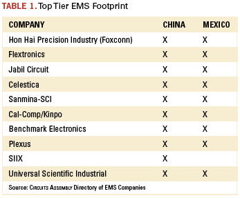
“The composition of the EMS markets in China and Mexico are quite different,” according to the CBA report, China vs. Mexico: An Objective Comparison for Midmarket Electronics OEMs. “While the Chinese market is comprised of both indigenous and global companies, Mexico is comprised almost exclusively of non-Mexican service providers primarily from the United States.” Table 1 shows the top 10 EMS companies from 2011 and whether they have a facility in China or Mexico.
For mid-market EMS providers, though, it’s expected that EMS production in Mexico is increasing and will continue to do so, according to CBA. The past decade saw a dramatic shift in electronics manufacturing to China in pursuit of lower assembly costs, including for LV/HM (low-volume/high-mix) assemblies. But CBA and others have documented a growing return to a regional approach by some North American-based OEMs that is benefiting Mexico.
“Our research has identified a trend of electronic OEMs returning to a regional approach to their manufacturing,” states the CBA report. “Regionalization is defined as when OEMs build their product in the region into which their product will be sold. In other words, they choose to build in region for region.”
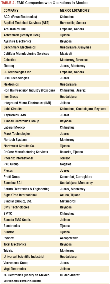
The number of EMS companies operating in China, both indigenous and foreign owned, is still too vast to list, according to CBA. The list of EMS in Mexico in comparison is fairly short (Table 2). (This is not an all-inclusive list, but does reflect what CBA believes to be the vast majority of EMS companies currently operating a facility in Mexico.)
EE Tech produces two-thirds of its sales volume at Empalme and about one-third of it in Reno. This is about 90% of unit volume in Mexico – more than 6 million printed circuit boards per year.
Newman says EE Tech chose Mexico because it was “looking for a solution that was going to be a price leader in North America not competing with the 10,000-plus shops already set up in Asia.”
“Our customers usually do not compare us to Asia. If they want Asia, they go there, as there are still some advantages if your supply chain is steady and large. However, if our customers are looking for some sourcing in North America that comes close to Asia pricing and better than the United States, Mexico is a great fit. Not only is it very competitive, it also is just a couple of days away via ground shipment, and none of our customers have more than a three-hour time difference. The staffing and technical expertise is an added bonus.”
Pros and cons. Ultimately, leading EMS providers weigh multiple factors before expanding operations in either China or Mexico. Sometimes, comparing the pros and cons of each location requires exceptional considering.
For example, Creation Technologies sees Mexico as a viable option, but has some concerns. “We would certainly look at Mexico as a manufacturing location,” Besse says. “Since we are focused on a niche market, we are seeking the right location. Because we are a private company, we are more cautious about entering Mexico these days, but the interest is definitely there.”
Creation’s supply base is 65% North American, 30% Asian, and 5% from elsewhere. Despite the fact that most of its suppliers are in North America, the company’s desire for an eventual Mexican location is customer-driven.
“Depending upon the customer and how they structure their manufacturing, it can be cheaper to build in North America. It’s not as simple as saying, ‘We should just buy it in Asia.’”
Creation Technologies provides services for high-mix, high-complexity, medium-volume electronic assemblies or total box builds (all commercial). The company’s customers are primarily North American OEMs looking for manufacturing services for North American or overseas markets. Besse says a growing segment of customer OEMs want to get their products into Asia, mostly China, because Asia by far is the largest market opportunity –but the bulk of customer products are still built and purchased in North America. A Mexico location would provide those customers with access to a Western hemisphere low-cost manufacturing area; lower shipping costs, and a more favorable time zone – but it still comes down to the importance of those factors in the OEM’s overall strategy.
“Are those issues of time and distance so overpowering that I can’t overcome them, or do I have the process and people to deal with it? Many OEMs will say, ‘I have an office in Asia already, and I am prepared to deal with the complexity because Asia.’ Looking at it from a cost point of view, Asia is still less expensive than Mexico. The labor-cost gap is steadily shrinking, and most likely will continue to do so over time, but as of this moment, when you do a straight comparison of manufacturing from a cost standpoint, Asia is the leader.”
Mexico: growth opportunity. Despite the attractiveness of a growing market in Asia, Mexico represents a growth opportunity for Creation because of its commercial niche, and when safety is no longer a concern, the company likely will establish a location in Mexico.
“In the past, companies have moved manufacturing to China because of cost savings, and on the consumer side, I don’t think we’ll ever see it come back,” Besse says. “However, on the commercial/industrial side, the cost of Asia versus Mexico and even North America, that gap is closing. We are also very interested in looking at the shelter business model that is available to companies that manufacture in Mexico. Using such as service provider is not a possibility in China.”
China is still a huge growth market, he says, but some customers are bringing products that they moved to Asia years ago back to North America because it is now no longer economically feasible to produce them there profitably.
The CBA research concludes that neither China nor Mexico provides a full-service solution across the manufacturing life-volume continuum, and each is best suited for specific manufacturing processes, but with one distinct difference: “Volumes appear to matter more in China than Mexico.” As way of qualification, Barnhart quotes one respondent’s description of the optimal build volumes in China: ‘The volumes need to be minimum revenue of $3 million to get into a decent Tier 2 EMS, and above $10 million for consideration at a Tier 1 EMS.’”
CBA has documented that the regional approach is “gaining traction, as this approach is now more cost-effective than a cross-hemispheric solution. The only known remaining exceptions are the extremely large consumer, communication and computing sector relationships, which are now atypical to the balance of the EMS/ODM industry.
“The return to regionalization, which is how the outsourcing industry actually began, should continue to benefit Mexico, especially in serving North American-based OEMs and also global OEMs that are selling their products into the North American market. Clearly this is influenced by the type of products, location of end-markets, and volume levels as mentioned above.”
EE Tech’s Newman says the company’s Empalme location in The Offshore Group’s Bella Vista Industrial Park is definitely part of the company’s future growth strategy.
“We still will primarily do all of the upfront prototyping, engineering, purchasing, and planning out of our Reno facility, but we will use our Empalme site to produce the volume at an economical North American price. Most of our new customers are coming to us because they ultimately want to use our Mexico price for volume builds.
“The hidden benefit to this is that we do most of all of the procurement of parts, planning, finance, customer service, and logistics out of the Reno facility, which ultimately creates business and jobs in Reno. I feel that if our Mexico facility did not exist, we would probably have about 75 Reno employees instead of the 150 that we have today. Operating in Mexico under a shelter plan has allowed us to successfully bid and take on volume work that we might have otherwise had no shot at winning.”
Tonya Vinas is a freelance writer.

Press Releases
- Zollner Puts a New Mechanics Building into Operation
- Changes in Incap’s Management Team: Incap updates its leadership model to support its growth strategy
- Niche Electronics Celebrates Completion of Florida Expansion
- Microscreen Names Nik Thomas Director, Expands Leadership Role Amid Continued Organizational Growth