

The EMS/repair depot/training center keeps rolling on.
Many are the number of successful companies launched in the founder’s garage. BEST got its start – literally – in a motor home.
It’s not how most executives would draw up their business plan, but that’s exactly how – or would that be where? – the now 16-year-old EMS company was launched: in a converted Winnebago.
The number of models for Tier IV EMS companies borders on infinite. Some offer straight consignment contract assembly. Others add turnkey services. Some specialize in repair. A few provide training certifications. Some have even ventured into distribution. That’s all in addition to the traditional work of assembling circuit boards, of course.
BEST (the acronym stands for Business Electronics Soldering Technologies) is one of the few that stretches the model in several directions, yet manages it so efficiently. The company still retains a sense of balance and focus. The firm takes a three-pronged approach, offering repair and reballing on a short-turn basis, training to IPC standards, and, most recently, an emerging turnkey EMS prototype-oriented operation. And it has diverged even further by developing its own line of dedicated rework stencils.
All of this takes place in a 24,500 sq. ft. building in Rolling Meadows, IL, just minutes from Chicago’s O’Hare International Airport. From the front, an otherwise nondescript building belies the flurry of activity going on inside. Inside, with three fully functioning businesses, space is at a premium.
Training has long been a steady business. The company is a Master Certification Solder Training Center for IPC-A-610, J-STD-001, IPC/WHMA-620 and IPC-7711/7721, and offers custom classes in SMT and rework.

New classes include ones for package-on-package (PoP) and thin silicon vias (TSV). Other non-standard courses include a five-day workshop on how to build a board, and classes on leadless device rework and profiling. BEST has developed its own test vehicles in order to ensure it matches real-world conditions. “We try to keep on top of the technology,” explains Bob Wettermann, chief executive and president of BEST.
At the Rolling Meadows site, it maintains a classroom with 10 stations for onsite instruction, but most (85%) of its training revenue is generated at remote locations. The company says it trains about 120 students a month, with an emphasis on methodology, not equipment. It boasts four trainers, all of whom are IPC Master Instructors.
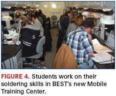
The Winnebago was launched as a Mobile Training Center (MTC), a door-to-door service provider equipped with soldering equipment, stereo zoom microscopes, and all the presentation bells and whistles one might find in its Rolling Meadows classroom, a brick-and-mortar site. The firm’s expertise in training comes in part from its own in-house experience. Roughly 20% of BEST’s floor space in Rolling Meadows is dedicated to contract rework and repair. The company primarily uses Metcal QX2 and APR/5000 rework stations, I&J Fisnar dispensers, and Leica microscopes, supplemented by a pair of SRT 1000 repair machines. Component rework runs the gamut from BGA to more complex bottom-terminated components such as QFNs and LGAs. It handles repair orders numbering from a single board to thousands of pieces, fixing anything from video game boxes to Class 3 flight controls. A large repair order would be 150 to 200 pieces, but for component reballing, some orders run in the thousands.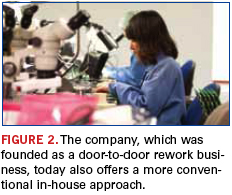
BEST also has a full complement of testing and failure analysis equipment, including hi-pot, functional and electrical test, and diagnostic test. Other gear includes GenRad X-1525 x-ray.
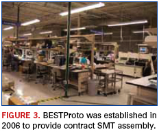
In 2005, the firm added BESTProto to handle higher board volumes. Garth Cates, previously director of business development for EMS firm AG Communication Systems and an engineer with Lucent, was brought aboard to manage the new organization’s sales. The plant features MPM SPM screen printers, Mydata MY19 and MY100 pick-and-place machines, Vitronics Soltec XPM2 and XPM520 reflow ovens, and a small SnPb wave. Nordson YesTech AOI, a Camelot glue dispenser, a Grieve oven, and an Aqueous Technologies SMT 400-CL batch cleaner round out the equipment list. (Conformal coating jobs are sent out.)
“If there’s a word that describes BESTProto, it’s flexible,” says Cates. According to Cates, BEST conducts “a lot” of process development for customers.
Between the two companies, BEST has 36 fulltime employees. The firm is ISO 9001-2008 certified and also strictly follows ITAR procedures in order to maintain its registration: A certain Circuits Assembly reporter was relieved of his phone while touring the building.
BEST is one of only a few companies that offer contract rework, SMT assembly services and IPC training. But perhaps where BEST truly deviates from the Tier IV model is in its line of patented and branded products. They include everything from repair kits to rework stencils and preforms.
The repair kits are straightforward and include tools for fixing lands, traces, gold fingers, plated through-holes and board substrates. In addition to the equipment, the kits include “how to” instructional slides and videos on its website.
The stencils were sophisticated responses to market needs. They started with BGA rework, when the firm developed the StencilQuik, which reduces the time required to rework BGAs while repairing mask damage. A year later, in 2007, BEST announced the launch of the EZReball, a preform that simplifies the reballing process by eliminating the need for custom fixtures or frames, and holds solder balls in place until after reflow, then peels right off. In 2010 came the StencilMate, a line of polyimide stencils that “bump” leadless devices for easier placement. Also in 2010, the company invented the StikNPeel rework stencil, which is designed for tight spaces, and is ideal for reworking connectors and QFPs.
“All our products come from solving customer problems,” explains Hung Hoang, operations lead, BGA and Products, who invented the rework stencils. “EZReball is one of the products we sell. StencilQuik and StencilMate were solutions to a problem.” Such products undergo traditional evaluation and testing. “We test it out first, then send to a customer to beta test and to get feedback,” Hoang says. A NASA/DoD study recently demonstrated StencilMate performs at the same level as traditional board paste printing, while also holding up under thermal shock and vibration testing.1
It’s been a lucrative development; today, the company’s own product line is responsible for about 25% of its revenue.
It can be hard to live up to a name like BEST. Wettermann, who bought the company in 2002, has led a 10-year run of expansion into new markets and buildings, not to mention revenue growth, but clearly maintains his inner geek, sharing anecdote after anecdote about running the business, but getting most excited when one of his colleagues brings forward a complicated fix for a customer or an in-house invention.
As for the Winnebago, BEST donated it a few years ago to a California-based company that teaches PC skills to the underprivileged in San Diego and has replaced it with a larger, yet more economical, diesel-powered truck-based unit. It’s fitting for a company that, after 16 years, is still on the go.
References
1. Bob Wettermann, “Simple, Fast High-Reliability Rework of Leadless Devices,” CIRCUITS ASSEMBLY, August 2012.
Mike Buetow is editor in chief of CIRCUITS ASSEMBLY (circuitsassembly.com); mbuetow@circuitsassembly.com.
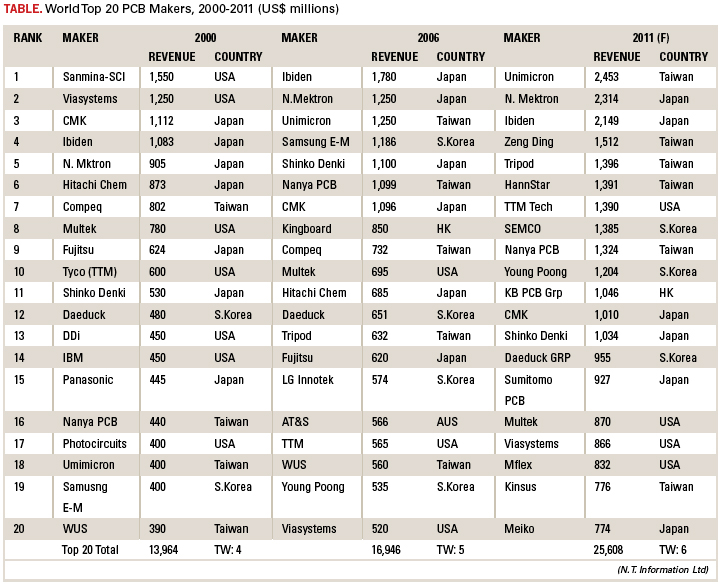
The 104 manufacturers on the 2011 NTI-100 made up more than 80% of the world’s PCB output.
The NTI-100 list for 2011 was greatly influenced by exchange rates. Taiwanese fabricators continued to make gains, followed by Japanese manufacturers. Some names disappeared because they were purchased; their sales are included in the acquiring firm’s results. Some disappeared because they did poorly. Several fabricators, particularly Japanese firms, made it because of exchange rates.
As usual, the author is not almighty and is certain that there are many errors. Some companies that should be on the list may be missing. He assumes full responsibility for any errors. He wishes to express his gratitude to those PCB makers that provided him valuable data.
Exchange rates. Currency values played a role in certain companies’ performance. Table 1 lists the average exchange rates of major currencies against the US dollar.
Assumptions. All acquisitions that took place during 2011 are assumed to have taken place on Jan 1, 2011. In the cases of flexible circuit manufacturers (FPC), the assembly value is included because it is extremely difficult to separate bare board sales from total revenues. Therefore, the rankings are relative, not absolute. Finally, a large portion of revenues of Taiwan, Japanese and US makers comes from overseas operations, and therefore involves double conversions. The author has no knowledge of what exchange rates Taiwanese makers, for example, used to convert output in RMB into NT dollars to report consolidated revenues.
Entries by country or region. There are 104 companies on the 2011 NTI-100 list. There are more Japanese makers than Taiwanese because of a 10% increase from 2010 to 2011 in value of the Japanese yen against the US dollar. Several Japanese makers would not have made it had the 2010 exchange rate remained constant.

Table 3 lists the 2011 NTI-100. Although comments are included in the table, more extensive comments on certain fabricators are below.
Unimicron. Unimicron purchased Ruwel International of Germany and Clover Electronics of Japan in 2011 and took in partial revenues of these two into its fiscal 2011 revenue. The revenue in the table takes into consideration full-year accounts of Ruwel and Clover. Unimicron is rumored to be shutting one of its Shenzhen facilities (“Plato”). It plans to build new facilities in Jining in Shandong Province and Nantong along the Yangtze River, north of Shanghai. Its 2011 output in China jumped by 60%.
Nippon Mektron. Its subsidiary, Mektec Suzhou, obtained water permission for its long-awaited second plant, which is undergoing construction. It is scheduled to commence operations in the fourth quarter this year. Its Thai subsidiary, Mektec Thailand, flooded badly, but most of the equipment was moved to higher floors and saved. It could restart production as early as December, and become fully operational by March. The company is expected to reach $3 billion in revenue in fiscal 2012.
Ibiden. Ibiden did poorly in flip-chip substrates for MPUs in 2011 due to sluggish PC shipments, but did very well with buildup MLBs for smartphones and tablets. It did well with IC substrates for baseband chips used for smartphones and tablets. It is reported that Ibiden is investing more than $2 billion to expand its overseas operations over the next three years, of which two-thirds will be used for PCB expansions. One-third of its fiscal 2011 revenue came from overseas production, but in fiscal 2013, Ibiden seeks to generate 60% of its revenue from overseas operations, particularly the Philippines and Malaysia. Its flip-chip substrate business is tops in the world, despite the slower 2011.
Zhen Ding. Zhen Ding is a business unit of Foxconn and was called Foxconn Advanced Technology prior to its Dec. 26, 2011, listing on the Taiwan Stock Exchange. A large portion of its revenue is said to come from FPC and FPC Assembly. The largest customer of its FPC business inclusive of FPC Assembly is said to be Apple Computer. It aims to become the largest PCB maker in the world in a few years, according to recent remarks by its CEO. It operates at two locations in Shenzhen, one at Yinkou, one at Qinghuangdao and one at Huai’an, all in China. Zhen Ding sold its Yantai facility to a business unit of Foxconn called Pan International prior to the stock listing because it was losing money, according to industry sources.
Tripod. Tripod’s revenue fell slightly in 2011 in terms of NT dollars due to poor PC demand. It has been reducing its dependency on the PC sector and diversifying its end-product markets. It is building new plants in Xiantao, about 100km west of Wuhan, along the Yangtze River. Two manufacturing buildings (of four planned) are nearly finished, and one will begin equipment installation toward the end of the third quarter and commence operations partially in the first quarter 2013. Automotive PCB is increasing at Tripod.
HannStar Board. HannStar Board completely absorbed GBM’s PCB units (GBM Yuanmao, CMK-GBM and GBM Chuangyi). GBM was building a facility in Chongqing. HannStar Board is trying to reduce its dependency on the notebook motherboard business. It made 93 million NB motherboards in 2011, mostly six and eight layers.
TTM Technologies. TTM is said to be strengthening its buildup MLB production capability both in technology and volume by adding a number of advanced laser drilling machines. Its US side of the business seems to be holding steady. Given the amount of investment in China, TTM’s future growth will come mainly from Chinese operations (TTM Asia Pacific, the former Meadville Technology).
Semco (Samsung Electro Mechanics Co). Semco benefited from high demand for Galaxy smartphones and tablets made by Samsung Electronics. However, 70% of its revenue came from IC substrates, flip-chip and wirebond types. Its Kunshan subsidiary, which makes buildup MLBs, also made a small contribution. In 2012, Semco is aiming at 1,900 billion won in revenue ($1.73 billion at 2011 exchange rates).
Nanya PCB. About $400 million of Nanya PCB’s revenue was derived from its Kunshan subsidiary, which has almost finished construction of a four-story PCB Plant 3 intended for wirebond IC substrates and for buildup MLBs. Nanya seems to be doing poorly in the first half of 2012, with a revenue decline of about 20% compared to the same period last year (parent only). Expected gains in the second half will hopefully compensate for a weak first half.
Young Poong Group. YP Group consists of Korea Circuits, Terranix, Interflex (FPC) and Young Poong Electronics (FPC). The combined FPC revenue of Interflex and Young Poong Electronics was $722 million, fourth largest in the world after Nippon Mektron, Sumitomo Denko Printed Circuits and M-Flex. Interflex’s gigantic eight-story building is completed in Ansan City, Korea, next to the head office of Korea Circuits. This plant will contribute greatly to the future revenue growth of YP Group. Buildup MLBs made by Korea Circuits are sold mainly to Samsung Electronics.
KB PCB Group. Kingboard Chemical’s PCB group consists of Elec & Eltek, Techwise, Evertek, Glory Faith, Top Faith and Express Circuits. Due to rising material costs and stiff price competition in the market, KB’s revenue was slightly below that of 2010. However, KB is in expansion mode, building huge plants for Elec & Eltek in Yangzhou (north of Nanjing), whose total production capability is planned to be 10 million sq. ft. per month when all five buildings are finished. Evertek in Kunshan is planning a four-story plant for buildup MLBs. Elec & Eltek Thailand was spared from the flooding last year. Top Faith seems to be building a new facility in Qingyuan, Guangdong Province.
Shinko Denki Industry. One of the major flip-chip package substrate makers (with Ibiden, Nanya PCB and SEMCO) for Intel chips, Shinko Denki, is building a major substrate plant in the city of Takaoka, Nagano Prefecture, for next-generation chips.
CMK. CMK’s revenue fell 10% in Japanese yen, but thanks to the rising yen, it remained in the NTI-$1B Club, which had 13 companies in 2011, up two from 2010. CMK was the largest automotive PCB maker in 2011, with revenue of $530 million, well ahead of No. 2 Viasystems. It expects that 60 to 65% of its revenue this year will come from automotive applications.
Daeduck Group. Daeduck Group consists of Daeduck Electronics and Daeduck GDS. Daeduck Electronics has two subsidiaries: APERIO, a maker of IC substrates, and Daeduck Electronics Philippines. GDS has a plant in Tianjing, which is rumored to be shut down. Its major customer is Samsung Electronics. Samsung is planning to ship 420 million cellphone units in 2012, of which 190 are to be Galaxy smartphones. Daeduck will benefit from this and is likely to join NTI-$1B Club in 2012.
Sumitomo Denko Printed Circuit. Several “Sumitomos” are engaged in the manufacture of PCBs: Sumitomo Mining (through a subsidiary, Shinko Mfg), Sumitomo Bakelite, Sumitomo Cable, Sumitomo Metal Electro Device and Sumitomo Denko. Sumitomo Denko has two FPC plants in Japan, two in China and one in Vietnam, about to be increased to two since it will be purchasing Sumitomo Bakelite’s Hanoi plant at the end of the third quarter. Forty-five to 50% of Sumitomo Denko’s revenue is said to come from sales to Apple.
Multek. Multek is a part of Flextronics and operates five plants in Zhuhai, China, one in Boeblingen, Germany, one in Sãn Paulo, Brazil, and one in Northfield, MN. Its FPC and rigid-flexible output seems to be increasing steadily, as is its high layer-count MLBs. Multek is a major buildup MLB maker in the world.
Viasystems Group. Some 48% ($412 million) of Viasystems’ bare board revenue came from automotive PCBs. It acquired DDi in May 2012, which will boost its military PCB output by several times. Its prorated revenue for bare PCBs in 2011 was $1.129 billion. Viasystems is one of the major high layer-count MLB manufacturers.
Multi-Fine Line Electronix. M-Flex sold its headquarters in Anaheim, CA, to DDi, which is now a Viasystems division, and moved to a new building in Irvine, CA. It used to have close to 400 employees in Anaheim, but is said to have only 50 now, with all other employees in China (Suzhou and Chengdu). Several years ago, over 80% of its revenue was from sales to Motorola. Now, more than 90% of its revenue comes from five major customers, including Apple and RIM.
Kinsus Technology. Kinsus Suzhou’s revenue contribution was next to nothing in 2011, but will be substantial in 2012, as its package substrate operations have been ramping since the beginning of 2012. Included in Kinsus’ revenue are sales from Piotek, formerly Boardtek, a subsidiary of Asustek. Kinsus PCB Group now belongs to Pegatron, a manufacturing arm of Asustek.
Meiko Electronics. Meiko sustained triple punches in 2011. The March earthquake/tsunami destroyed Meiko’s Ishinomaki plant, and the Fukushima plant was shut down for several months due to its proximity to the Fukushima nuclear plant, which exploded from the loss of its cooling pumps. Then, on Oct. 18, one of its two Wuhan plants was shut down for three months by Chinese authorities on suspicion of wastewater treatment violations, which was very much a political issue related to Apple’s suppliers (the “poison Apple” case, as the Chinese called it). The issue was resolved on Jan. 19, 2012. As a result, Meiko has been accelerating operation of its new Hanoi, Vietnam, plant. Despite all these problems, Meiko ended fiscal 2011 with a net profit. Meiko will see strong growth in 2012, with the Fukushima and Wuhan plants operational and the new Vietnam plant contributing greatly.
Compeq. Compeq has been doing well this year. It is one of the major PCB suppliers to Apple for all product lines (iPhones, iPods, iPads and iMac). Its Chongqing buildup MLB plant is scheduled to commence operation in the first quarter 2014.
Wus Group. Wus China was listed on the Shenzhen Stock Exchange in 2010. This China organization is separate from its Taiwan operation, but major ownership is common to both organizations. A new plant consisting of two buildings in Kunshan, about 20 minutes from the existing plant, is nearly completed, with total floor space of 2 million sq. ft. A second plant is in planning at Huangxi, 100 km east of Wuhan. Wus is one of the major high layer-count MLB makers in China. Of the $468 million revenue generated at Kunshan, well over $100 million came from MLBs above 18 layers.
AT&S. AT&S is Europe’s largest PCB maker, but the majority of its output came from its Shanghai plant ($403 million, or 56%). AT&S is also a major producer of automotive PCBs, with 2011 revenue of $120 million. It has been building a gigantic buildup MLB plant in Chongqing since July of 2011, and the building seems almost complete. It is scheduled to commence operation in early 2013. AT&S took a technical license from Panasonic to manufacture “ALIVH” products.
Fujikura. Fujikura is a major FPC manufacturer. Unfortunately, 95% of its output came from three plants in Thailand, two of which were completely flooded in fall 2011. One of the plants started partial operation in May, and the other is scheduled to restart operation in December, according to the company’s annual report. In the meantime, Fujikura purchased an FPC plant in Vietnam from bankrupted Sakai Denshi last December and commenced operation in January. At the same time, Fujikura selected land in Thailand high above sea level to build a new flex manufacturing plant, which is supposed to generate 30% of future revenue.
Gold Circuit Electronics. GCE is the second largest notebook motherboard maker, after HannStar Board. Unfortunately, its main notebook motherboard plant in Changzhu, China, had a fire and was disabled for some time. It has been restored.
Simmtech. Simmtech used to be Chungbuk Electronics. When it started to enter the single-in-line memory module business, it changed its name to Simmtech. In the last several years, Simmtech has been growing rapidly in the IC substrate market as well. It built a plant in Xian, China, to supply memory module circuits to Micron and Samsung Electronics.
Nitto Denko. Nitto Denko is a major Japanese FPC maker with plants in Japan, China (Suzhou) and Vietnam (near Ho Chi Minh City). It is building a new plant next to the existing plant in Vietnam.
Chin Poon Industrial. Chin Poon has several plants in Taiwan and a plant with two buildings in Changshu, China. It is the third largest automotive PCB maker in the world, with $300 million automotive revenue. Its Thailand subsidiary (minority share) was badly damaged by the flooding in the fall of 2011, but is fully restored.
Unitech Electronics. One of the largest buildup MLB makers in the world, Unitech built a new buildup plant in Ilan, Taiwan, which started operation in 2011. It has a provision to build a plant near Nanjing, but no concrete plan is set at this time, it seems.
PID (Panasonic Industrial Devices). Formerly Panasonic Electronic Devices, and inventor and licensor of ALIVH technology, PID built a second ALIVH plant in Taiwan (Tayuan) and another ALIVH plant in Vietnam (Hanoi). Its overseas ALIVH production capability will triple when these two new plants become fully operational this year.
LG Innotek. It is said that LG Innotek supplies over 80% of its output to its parent, LG Electronics. Since LGE did poorly in cellphones in 2011, LG Innotek also did poorly. It decided to exit the high layer-count MLB business in 2010, which is a shame because it had very high technology in this field. The reason for the exit is that the market for high layer-count MLBs is rather small and is not growing compared to other fields such as IC substrates and buildup MLBs. So, now, LG Innotek concentrates on IC substrates and buildup MLBs. It supplies buildup MLBs (“any layer” type) for Apple’s smartphones.
Founder Technology. Owned by Beijing University, Founder Group went into the PCB business in 2004 when it purchased Zhuhai Multilayer. Since then, it acquired a quickturn and prototype maker in Hangzhou and built two new PCB plants: one in Zhuhai and the other in Chongqing. Zhuhai “Fushan Branch” plant in Doumen district of Zhuhai consists of four operations: buildup MLB, QTA and prototyping, R&D and IC substrate. The last operation is called ACCESS (Advanced Chip Career Electronic Substrate Solutions). ACCESS is a JV between Founder and Israeli substrate maker Amitek. (ACCESS’ revenue – $70 million in 2011 – is not included with Founder’s.) Founder built its second buildup MLB plant next to its existing site early this year and a separate quickturn plant at its Zhuhai Fushan Branch last year. Founder is one of what the author calls “three musketeers of China,” the others being CCTC and Shennan Circuits.
Shennan Circuits. A division of AVIC Group (Aviation Industry of China), which makes jet fighter airplanes, helicopters, automobiles, missiles and jet engines among other things, Shennan Circuits is one of the China’s best high layer-count MLB builders, with two plants in Shenzhen (Nanshan and Longgang districts). In 2011, it commenced production of BGA substrates and has been negotiating with Wuxi government to build a new BGA plant there.
China Circuit Technology Corp. CCTC is one of the large makers of buildup MLBs for local cellphone makers. CCTC has two plants in Shantou, Guangdong Province, a small plant in Shenzhen and another small one in Shichuwan Province. CCTC belongs to Go-World Group, which also has a laminate manufacturing subsidiary.
DDi. DDi, the second-largest PCB maker in North America after TTM, was purchased by Viasystems Group in May. This purchase boosts Viasystems’ military portion of its PCB business to well over $100 million.
Wuzhu Group, Shenzhen Fast Print, Shenzhen Sun Tak and Bomin Electronics. These three makers may be called second tier “four musketeers of China.” All have substantial expansions ongoing in various parts in China: Wuzhu in Dongguang, Fast Print in Yixing, Suntak in Jiangmen and Bomin in Meizhou.
Tat Chun Circuits. Some 51% of Tat Chun was acquired by Korean high layer-count MLB maker ISU Petasys in May of this year. “ISU” in Korean means “Pear Tree, or 梨樹. Peta is 10 to the 12th. The parent company, ISU Chemical, named it as Petasys to wish that it would grow to “infinity.” Tat Chun has had a business alliance with Japan’s Toppan-NEC, a competitor of ISU Petasys for Cisco’s programs. ISU Petasys is the largest supplier to Cisco. What is going to happen with Tat Chun, Toppan-NEC and ISU Petasys is beyond this author’s imagination. Good luck to all parties involved.
Ed.: For a larger version of Table 3, right-click on each table, then click View Image and increase the size.


If readers have questions about other NTI-100 entries, the author would be happy to respond.
One final comment: The “80-20” rule normally applies to the amount of market share controlled by 20% of the manufacturers in the same field. It is estimated that there are 2,600 to 2,800 PCB companies in the world today. The 104 companies on the NTI-100 list represent 3.7% of the total. The total revenue ($48 billion) of these 104 makers accounted for 81% of the world output ($59 billion). Therefore, in the PCB field, the rule may be more like “90-10”; that is, the big get bigger and faster.
Once a PCB manufacturer’s revenue reaches a certain level, say, $500 million per annum, it must keep running, meaning continuous investment. Some companies are taking a different path, specializing in a niche market with niche products. Which is better?
Ed.: To see the 2011 NTI-100, click here.
See below for a list of the world's top PCB fabricators over the years:
Dr. Hayao Nakahara is president of N.T. Information; nakanti@yahoo.com.
Follow us on Twitter: @mikebuetow
Steps for saving money through awareness and tighter process control.
Electronics manufacturers have many potential impacts to the environment. Here, we provide a methodology to identify and institute controls to mitigate negative impacts to the environment. Environmental impacts will be different between manufacturers, but the goal is the same: to identify, control and improve.
Identify. An environmental impact will be defined as a process, material or activity that interacts with the environment. The first action is cataloging, reviewing the facility’s manufacturing processes, materials, products and services to determine which activities impact or could potentially impact the environment. Sourcing of information for compiling this list typically includes:
- Facilities’ environmental permits and reports.
- Material and chemicals that are hazardous or used in volume within the facility.
- Air emission processes and equipment.
- Generated waste, nonhazardous and hazardous.
- Materials, products and items that can be recycled.
- Energy use.
Some examples of environmental impacts are lead or lead-free solder, manufacturing chemicals, hazardous waste, recyclable materials, including manufacturing materials and non-manufacturing materials such as bottles, cans and metal.
One of the best approaches is to audit the facility and determine what is being thrown out as waste. Investigate if any of the items can be recycled. Recyclable packaging materials such as cardboard, paper, metals might otherwise be discarded without understanding the negative environmental impact.
Controlling the environmental impact. Upon identifying and listing the environmental impacts within a facility, the next stage is controlling the process, material or activity. The control may be different given the specific impact, with the main goal being to eliminate the opportunity to adversely affect the environment.
Controls may not be needed for some impacts; these would require improvement as detailed in the next section. Table 1 lists some examples for controlling the impact.

Some chemicals are considered as hazardous waste and should be disposed of per federal and state guidelines. For chemical spills, control procedures may be required per state and federal guidelines dependent on the specific chemical, and if determined to be hazardous or regulated by the EPA.
When controlling environmental impacts, consider health and safety of the employees and wearing the appropriate personal protective equipment (PPE), such as gloves, eyewear and clothing. These PPE guidelines are listed on the material safety data sheet (MSDS) for the specific chemical and material.
Improve. Some environmental impacts within a facility may not require controls because the absence of controls will not impact the environment directly. Nevertheless, these impacts should be continuously improved. Recycling opportunities and energy use are two areas that if improved could help the environment.
Recycling opportunities. Opportunities exist, the first being glass, plastic bottles and aluminum cans. The next major opportunity is commingled fiber, which includes cardboard, printer paper, newspaper, magazines, notebooks, etc. Conduct an audit of what is being discarded at the facility as waste; some items may be recyclable, saving waste from the landfill.
Electronics assemblies, subassemblies and individual components may also be recyclable; the determination requires diligence before being deemed recyclable, given hazardous substances and state regulations. Solder dross (lead and lead-free) is one example of material that may be recycled, given its characteristics and metal content.
Other opportunities within a typical manufacturing facility include computer equipment and scrap metal, such as piping, tooling and fixtures. Including the environmental benefit of recycling, a cost payback may be received given the item and supplier. Typically, solder dross and metal will have the two highest paybacks.
Energy use. Most electronics manufacturing facilities have many opportunities when trying to reduce energy use. A few of the main areas to investigate and improve are lighting, equipment and motors. Lighting can be addressed by upgrading fixtures and lights to high-efficiency equivalents and determining if certain areas of a facility can be shut off when not in operation.
Equipment is similar to lighting; determine if the specific piece of equipment can be turned off to save energy. This may make sense for some machines, but not for others. A wave solder machine or a plating bath, for instance, can take several hours to reheat the metals. Given the time it takes and manufacturing build requirements, it may not make sense to switch off such equipment.
Motors are used throughout every facility and are often overlooked. Older motors with higher horse power use the most energy. A new high-efficiency motor will save on energy and may have a payback of less than one year, especially if rebates are available by your local electric company. With any energy project, calculate the cost savings and time to payback the cost of upgrading.
By identifying impacts as detailed above, an operation can deploy controls to eliminate or significantly reduce the impact to the environment. Many opportunities exist within a facility to recycle or for energy reduction. Both help the environment and can result in cost paybacks or reductions.
Bibliography
1. Scott Mazur, “Benefits of an EMS for the EMS,” CIRCUITS ASSEMBLY, August 2011.
2. Scott Mazur, “Environmental Recycling for the EMS,” SMT, October 2010.
3. Sammy Shina, Ph.D., ed., Green Electronics – Design and Manufacturing, McGraw-Hill, 2008.
Scott Mazur is a manufacturing staff engineer and environmental management representative at Benchmark Electronics (bench.com); scott.mazur@bench.com.
The EMS market continued its extraordinary growth surge.
The worldwide contract electronics manufacturing market made another large jump up in 2011, increasing nearly 12% in revenue, following an extraordinary 2010 in which the industry expanded by 37%. Whereas most industry observers expected a modest growth rate in 2011, no one anticipated this strong a market, which was driven by continued demand for smartphones and new mobility devices (iPhones, iPads and e-readers). The largest beneficiary of this growth was Foxconn, the dominant subcontractor of these devices for a variety of key OEMs. Provided Apple continues its spectacular growth in revenue, as most analysts predict, Foxconn will continue to be lifted by its customer’s rising tide.
The really good news is that virtually all industry participants made money in 2011, with very few exceptions. In fact, the contract manufacturing industry made more money in 2011 than at any time in history, although this may not continue if the past is any indicator. Foxconn once again set the record ($2.7 billion, not a great result given its total revenue of $111 billion), followed by HTC ($2.1 billion), and to a lesser extent a number of Asian ODMs. Only a minority of EMS firms did not grow or make money in 2011.
Figure 1 presents the summary forecast for the worldwide revenue growth of the EMS market from 2011 to 2016. Given the minor differences in business models between EMS firms and ODMs, NVR foresees little separation between the two types of suppliers with regard to customer services and revenue growth. ODMs should underperform EMS companies over the forecast period as a result of a riskier business model that relies on giving preference to branded and low-end computer, communications, and consumer products. To their credit, ODMs are usually better able to streamline their production methods and create economies-of-scale through the concentration of components and vertical integration, but ultimately all profits get driven to the margin over time. Because EMS firms manufacture a wider range of products, and can leverage their operations in different ways, it is believed that they will experience a slightly higher growth rate over the forecast period.

The shift in production to low-cost regions has been fully accomplished over the past several years. Today, we are seeing OEM customers requiring their EMS partners to manufacture products near the regions where they are to be sold. For certain high-volume products like mobile phones and PCs, OEMs need to leverage the lowest cost in manufacturing. However, for other products the labor cost differentials are becoming less significant when weighed against the total cost of production (including transportation and logistical challenges). Offshore product migration will still take place, according to NVR’s forecasts, but it will be at a more moderate pace.
Both EMS firms and ODMs will experience strongest growth from production in the communications, computer, and consumer market segments. Specifically, EMS companies will find very strong growth in e-readers, tablets, enterprise storage systems, and personal navigation systems, while ODMs are projected to experience very strong growth in tablets, e-readers, cellular handsets, notebook PCs, and digital cameras. In general, EMS firms will tend to excel in technology-intensive product areas and complex board assemblies, while ODMs will excel in manufacturing commodity/high-volume products such as motherboards, monitors, handhelds, and consumer electronics.
Foxconn continued its extraordinary dominance as the leading EMS firm in the industry, outdistancing its closest contender by more than three times in terms of revenue. Flextronics remained steadfastly in the No. 2 position, followed by two ODMs (Wistron and Quanta Computer), and Jabil Circuit (Table 1).

Every year, New Venture Research conducts a financial and performance comparison and ranks the top 10 overall best-performing EMS companies. In 2011, HTC emerged as the EMS provider with the highest ranking score, followed somewhat distantly by Quanta Computer and Wistron, according to NVR’s metrics. Note that all of these high-performing companies were Asian ODMs. Jabil Circuit scored a respectable fourth in the rankings.
NVR has just published its market research study on the contract electronics manufacturing services market in a report titled, “The Worldwide Electronic Manufacturing Services Market, 2012 Edition.” More details can be seen at newventureresearch.com/wp-content/uploads/2012/06/ems2012-RS.pdf.
Randall Sherman is president and principal analyst of New Venture Research (newventureresearch.com), a market research and consulting firm specializing in the electronics manufacturing industry; rsherman@newventureresearch.com.
Long relied upon for component ESD qualification, the machine model is being rapidly discontinued, and for good reason.
The Machine Model test, as a requirement for component ESD qualification, is being rapidly discontinued. Here we illustrate why MM evaluation is not necessary for qualification. The following major conclusions can be made about MM in general:
- MM is redundant to HBM at the device level since it produces the same failure mechanisms, and the two models generally track each other in robustness and in failure modes produced.
- The MM test has more variability than HBM due to the MM’s greater sensitivity to parasitic effects in the tester circuitry.
- There have not been any significant engineering studies (with verified data) that could be used to establish required passing level.
- The test method was incorrectly given the name “Machine Model,” although no firm, unique connection between the model and actual machine-induced device failures has ever been established. In fact, the model was developed as a “low-voltage HBM.”
- CDM does a better job of screening for fast metal-to-metal contact events than MM.
- The vast majority (>99%) of electrical failures in manufacturing correlate to CDM and EOS, not MM.
- MM testing has not shown any additional failures not explained by CDM, HBM or EOS.
- MM testing consumes resources and creates time-to-market delays, while providing no additional failure modes or protection strategies that HBM and CDM already cover.
- It is important to understand the scope of this memorandum. It summarizes what has been learned about the test method only. The information summarized here in no way diminishes the importance of adequate grounding of any metal that may come in contact with ESD-sensitive devices and the importance of the avoidance of hard metal-metal discharges.
Background. The Machine Model (MM) is a widely misunderstood component ESD qualification test method. It continues to generate confusion for OEM customers and their IC suppliers during ESD qualification. Many companies and design organizations continue to use MM, mostly as a legacy “required” practice, despite the fact that it has been downgraded by three standards bodies and is no longer recommended for qualification testing in accordance with Jedec JESD47. The automotive industry, a longtime user of this method, no longer requires it in their AEC-Q100 list of qualification tests. The scopes of the Jedec (JESD22-A115) and ESDA (ANSI/ESD STM5.2) test method documents have also been changed to reflect this status. There are a number of reasons for these changes, as will be outlined below. The continued use of MM for qualification based solely on legacy requirements has no technical merit, given the information that has been gathered over the past few years. Those companies that continue to use MM will take on an unnecessary and burdensome business approach. The reasons against use of the MM are below:
- Historically speaking, the 200pF, “0Ω” model, later known as the machine model, originated from several Japanese semiconductor corporations as a worst-case representation of the Human Body Model (HBM). The model was later presumed by some, because of the lower discharge impedance, to simulate abrupt discharge events caused by contact with equipment and empty sockets (functional test, burn-in, reliability testing, pick-and-place operations, etc). This happened at a time when the very fast rise time of metal-metal discharges was not well understood. Since that time, the Charged Device Model (CDM) has been proven to quite adequately cover these events.
- Recently, Tanaka1 presented rationale and data supporting the elimination of the MM test. According to his historical account, the so-called Machine Model originated at Hitachi (now Renesas) about 45 years ago and was introduced to Japanese semiconductor customers as a test case to represent the HBM test in their IC product test reports. This test method spread widely to the Japanese customer base and was later established as an ESD test standard by the EIAJ in 1981. Around 1985, some began to mistakenly refer to the test as the Machine Model. Then, starting in 1991, ESDA, Jedec and IEC adopted the model and its name as a new test standard. As use of the model increased, it was realized that the Machine Model name caused misunderstanding that needed to be clarified.
- In the early days of ESD device testing, there was also a desire to avoid the high pre-charging voltages of the HBM test (2kV and higher), and the 200pF and low impedance of the “MM” was thought to be an equivalent but safe lower voltage test to address the same failure mechanisms as HBM. However, establishment of a single translation from MM voltage to HBM voltage has been difficult to achieve. Protection design has traditionally been focused on meeting the HBM requirement, but MM testers are susceptible to parasitic circuit elements; these parasitics from relay switching networks in the simulators cause more variation in the MM waveform than waveforms from HBM testers. In spite of this and without any supporting data, 200V MM became established as a de facto requirement. It was thought to be the safe level for handling and that this level had to be simultaneously met, along with the de facto 2kV HBM standard. In reality, a device with a 2kV HBM withstand voltage might have an MM withstand voltage anywhere from 100V to 300V, depending on the device characteristics and the MM tester parasitics. This led to much of the confusion associated with specifying both HBM and MM specification levels.
- The next important reason for discontinuing MM is that fast discharges to or from a metal surface are not correctly represented by the MM. The characteristics of the MM rising pulse were not established based on comparison to measurements on machine pulses, but rather were determined by characteristics of the already developed HBM simulators. The fast rising leading edge of metal-to-metal discharges is actually more effectively simulated using the current standard CDM test methods. This is known today because of the development of high-speed oscilloscopes. However, during the 1980s, there was a misunderstanding that MM was a good representation for CDM. This misunderstanding actually delayed the eventual development and acceptance of the CDM standards used today. In the 1990s, with the much improved and accurate test for CDM and wider recognition that the fast discharges are covered by CDM alone, the test for MM became more frequently replaced with CDM.
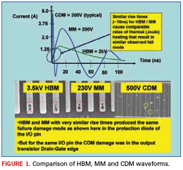
MM vs. HBM and CDM. The waveforms for HBM, MM and CDM are compared in Figure 1. The HBM and MM have similar ranges of rise time (2 to 10ns). Therefore, any thermal heating in silicon taking place in this time period leads to the same failure mechanisms for both models. This holds true for all technologies, including advanced technology nodes. This early part of the waveform determines where protection circuits must be deployed in design. With similar rise time characteristics, HBM and MM encourage the same protection designs. For CDM, on the other hand, the rise time is much faster (0.1 to 0.5ns) and often leads to a unique failure mechanism like oxide breakdown. Even more important, the observed ESD field failures are dominated by oxide breakdown when the CDM level is not adequate. Thus, a different set of protection strategies are generally needed for CDM. This makes it more critical to focus on CDM qualification, instead of duplicating the HBM test information by using the MM. Figure 1 shows the observed failure modes for the same I/O pin after stressing with HBM, MM and CDM. It is clear that with HBM and MM, the damage sites were the same, in the protection diode, but with CDM stress, the damage site corresponds to oxide breakdown in the output transistor. This also illustrates that meeting high levels of MM does not improve CDM performance until the right effective design techniques are employed.
Commercial MM testers have inductors built into the MM stimulus circuit. These inductors must be present to produce the oscillatory waveform required in the MM test method. The inductors, however, actually slow the MM waveform (Figure 1), and therefore, MM cannot represent very fast metal-to-metal contact discharge as CDM does. On the other hand, the CDM test is directly represented by elevating the package potential and directly grounding the pin to produce the fast discharge. MM cannot be relied on to accurately model fast metal-to-metal contact discharges, which are known to occur in the field.
Metal discharge vs. CDM discharge. Analysis of Tanaka4 is shown here to demonstrate that a metal discharge from a small metallic object to a device is similar to the commonly used CDM test. Tanaka considers small objects because large machines (typically >10pF) are almost always grounded for reasons beyond ESD and thus pose little practical threat for these events. On the other hand, tools and small machines are difficult to ground and may lead to charging effects, where the capacitance of the metal object is related to surface area and distance. These values can range from <1pF to nearly 10pF. For example, this could be as much as 1pF for a small metal object of 10cm2 at a distance of 0.5cm. Both the small metal discharge and the CDM discharge can be represented by the same set of equations for I(t), and thus both can be expected to generate the same discharge event if the values of the parameters are similar. Figure 2 illustrates the case for a small object of 10pF for both metal discharge and CDM discharge.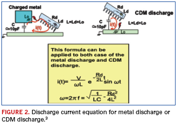
The above analysis is confirmed by measurements3 (Figure 3) where the discharge (a) from a charged tweezer to IC pin is the same as direct discharge from metal as shown in (b), and both are similar to the generated CDM discharge in (C). The time scale for both metal discharge and CDM discharge are indeed the same, clearly indicating that CDM is a good representation of the metal discharge in the EPA.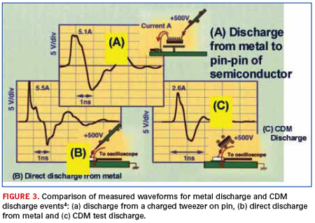
- Metal discharge events are well represented by the CDM test.
- Most of the field failure returns for ESD have been replicated by the CDM test, but none known with the MM test that are not also produced by HBM.
The Industry Council on ESD Target Levels has studied the HBM and MM results on a wide variety of designs in many technologies and has concluded that MM is intrinsically related to HBM, with a correlation factor “range” that is dependent on the HBM design level.2 These data are represented in Figure 4. However, the most important conclusion of the study was that MM is a redundant test and that a sufficient level of MM robustness is automatically included in an adequate HBM design. This also includes the bipolar nature of the MM stress. Any oscillatory waveform that might be measured during discharges in the field is sufficiently covered, if the part is proven to have an adequate HBM design.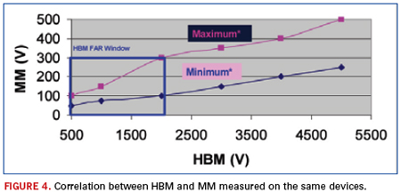
This minimum design value, as measured by an MM tester, is well above any voltage remaining on all properly grounded machines in an ESD protected manufacturing environment. In essence, meeting a safe value for HBM (and CDM) is sufficient for production of ICs without needing to evaluate MM as an additional qualification.
- The Machine Model test method specification to qualify ICs does not model or advance the real world ESD protection of IC products.
- IC evaluation with MM does not give any additional information as to how to address machine ESD control.
- While MM is an unnecessary qualification test, it is important to emphasize that control of voltage on machine parts that might contact device pins in accordance with ESD program specifications such as S20.20 programs is still important.
Field data analysis. The Industry Council work has shown that most of the overstress field returns exhibit failure signatures of higher energy EOS, and that the level of HBM ESD from 500V to 2000V (shown as the HBM Failure Analysis Return (FAR) window in Figure 2) on 21 billion shipped units did not show a correlation to the customer field return rates. Similarly, these very same shipped units (500V to 2kV HBM) also had MM levels in a range of 50V to 300V, as also seen from Figure 2. Therefore, it can be concluded that the EOS field returns are indeed not related to this range of intrinsic MM levels. That is, it does not matter if a shipped device has a measured MM value of 50V or 300V.
Devices with various measured MM levels have shown no correlation to real world EOS failure returns.
Standards bodies and positions on MM. During the past two decades, the electronics industry’s standards bodies have changed their viewpoint with regard to MM and its requirement for IC qualification. At present, JEITA does not recommend MM. The Automotive Electronics Council’s AEC Q100 standard gives a choice between HBM and MM, but does require CDM. In recent years, Jedec has strongly recommended discontinuing use of the MM for ESD qualification because of its test variability and non-correlation to real world failure modes. In general, standards bodies have come to recognize that:
- IC qualification to HBM and CDM provides all the necessary ESD test requirements.
- MM testing of ICs is redundant to HBM and does not reflect unique real world component ESD failure modes.
- Billions of IC components have been shipped worldwide and qualified using HBM and CDM testing only. No field failures have been found that would have been prevented by additional MM qualification.
The following statements are from the Jedec website:
- “JESD22-A115B is a reference document; it is not a requirement per JESD47G (Stress Test Driven Qualification of Integrated Circuits).
- Machine Model as described in JESD22-A115B should not be used as a requirement for IC ESD Qualification.
- Only human body model (HBM) and charged device model (CDM) are the necessary ESD Qualification test methods as specified in JESD47G.”
- The ESD Association has downgraded the MM document from a Standard (S5.2) to a Standard Test Method (STM5.2)4 and has adopted the following position: “The ESD Association does not recommend using MM ESD as described in STM5.2 for IC qualification. IC qualification should be done using the current standard HBM and CDM methods.”
Conclusions
The information herein supports the discontinuation of MM as part of IC qualification. Most important is that a wide range of products having only HBM and CDM testing performed are being shipped today at volume levels in the billions, with no field returns due to ESD. These products, passing at or above the recommended minimum HBM and CDM levels, are being routinely shipped by major suppliers, and are accepted by major OEMs. No increase in field return rates has been observed with MM removed from qualification for these products.
The confusion generated by MM has persisted for over two decades. The presumed need for this test is causing additional qualification delay due to an extraordinary consumption of design / test resources, added delays in time-to-market, and in some cases having an impact on IC speed and performance. Maintaining safe HBM and CDM levels is sufficient to meet all IC manufacturing, handling and assembly needs.
Different customer sectors may feel they need enhanced ESD requirements for specific reasons. For example, some automotive customers have more consistently required MM model testing, the impression being that an independent and redundant test provides enhanced safety, improved quality and reduced defectivity. However, industry experience has shown that passing a redundant (to HBM) MM qualification test does not help automotive manufacturers achieve these goals. Meeting current industry standard HBM/CDM will ensure that a product can be safely handled with sufficient margin to prevent ESD damage and maintain the quality/reliability of the product as shipped from the component manufacturer. Since many suspected ESD failures turn out to be higher energy EOS in nature, methods to prevent electrical overstress during manufacturing will also help maintain product reliability.
Common goals. We have presented evidence and arguments that the MM test of ICs is redundant, and there is no proof that devices have failed in the field because MM evaluation was not done. We strongly recommend that this test be discontinued for ESD qualification. This will save the semiconductor industry a tremendous and unnecessary burden by greatly reducing the routine characterization that is done to support the qualification process. The ESD robustness designed into integrated circuits to survive HBM and CDM testing will provide protection against any MM-like stress. Eliminating MM testing of ICs has no deleterious effects and will free up resources for more important engineering challenges.
References
1. M. Tanaka, JEITA/JEDEC Meetings, September 2011.
2. JEP155, “Recommended Target Levels for HBM/MM Qualification,” jedec.org and esdtargets.blogspot.com.
3. M. Tanaka, K. Okada and M. Sakimoto, “Clarification of Ultra-high-speed Electrostatic Discharge and Unification of Discharge Model,” EOS/ESD Symposium, 1994.
4. ESDA standards document definitions and hierarchy are summarized at esda.org/documents.html.
Ed.: This article is courtesy of the ESD Association (esda.org).
Charvaka Duvvury, Texas Instruments (ti.com); Robert Ashton, ON Semiconductor (onsemiconductor.com); Alan Righter, Analog Devices (analog.com); David Eppes, AMD (amd.com); Harald Gossner, Intel (intel.com); Terry Welsher, Dangelmayer Associates; and Masaki Tanaka, Renesas Electronics (renesas.com).
New tools are automating print and placement analysis without performance tradeoffs or retrofits.
To do their jobs on assembly lines, SPI machines generate huge quantities of valuable data that often go underutilized. The information they gather on deposit heights, volumes and locations to pass or fail a print can also be used for a variety of engineering purposes. Documented applications include print parameter optimization, paste selection, board support analysis, and stencil evaluation and verification. Many of these uses have been discussed in this series of articles (see editor’s note).
Until recently, application of the data has been based solely on the engineering department’s ability to utilize it – their intellectual, analytical and creative abilities, as well as their general availability in this era of Lean staffing. But that’s changing, as the equipment suppliers are producing new applications for the data, often at the behest of assemblers. These new applications are software-based and use the data generated during print inspection to automatically control and improve the overall SMT process.
Automatic print offset feedback to stencil printers. Measuring print offsets is anything but new; SPI machines have always measured print offsets, and those offsets could always be fed back to the printer – by a human.
It’s easy to query paste-to-pad alignment data through the machines’ SPC interfaces and use the information to tweak printer alignment when necessary. Historically, this had been a good, albeit inefficient, way to dial in the process to compensate for PCB shrink or lot-to-lot positional variation. The inefficiency stems from the need for human intervention; a person has to decide to query the database (in real time, not the next day), determine if an adjustment is needed, and then physically make the adjustment on the printer. Adding to the variability of this process, the person would need to query the SPC at critical times: for example, when different lots of PCBs reach the assembly line. So although the SPI systems have always provided powerful offset measurement capability, they historically relied on what is often the weakest link in a production system: the operator.
Eliminating the human element eliminates a major source of variation. Now, with the link between the SPI and printer completely automated, PCB assemblers can instantly realize more value from their inspection equipment. Small process deviations can be addressed before they grow into out-of-control situations, and SPC on PCB positional accuracy can actually serve as an early warning system for other bare board-related issues.
Automatic wipe triggering. Stencil underwiping is still a bit of an ambiguous science, despite all the technology that’s been applied to solder paste printing over the past two decades. Variables like wipe frequency, wet/vacuum/dry sequences, solvent selection, wiper design and paper quality all affect printer output, but are not studied nearly as often as items like print parameters, stencil designs or tooling supports. As an industry, we are largely uneducated about the nuances of the stencil underwipe process, often setting wipe parameters somewhat arbitrarily.
An automatic underwipe can be triggered by a number of print problems. Insufficient volumes may indicate clogged apertures, while excessive paste volumes, bridges or smears may indicate residual paste on the bottom of the stencil. In either of these situations, the underwipe is needed to remedy the issue and regain control of the process.
Automatically triggering the underwipe eliminates line downtime waiting for an operator to respond to a print failure, judgment calls on whether an underwipe is needed, and eventually, arbitrary guesses at what regular production wipe intervals should be.
Automatic placement adjustments. Feed forward controls can now communicate component positional offsets to the placement machines. As components get smaller or more complex, they become less forgiving to offsets or skews. Placement accuracy for 0201s, 01005s and certain bottom termination components like DFNs or QFNs is critical to end-of-line yields. The often unpredictable shrink (or stretch) in PCBs can now be captured at SPI and communicated to pick-and-place automatically, shoring up the PCB-induced slop in the placement process.
Just like print offsets, placement offsets could be queried at key times by humans and manually translated to the pick-and-place machines. Production line placement tweaks have typically been frowned on by our industry, because when they’re executed haphazardly, they can easily ruin the integrity of the placement program’s CAD data. Automatic adjustments, however, are more accurate than human ones, protect the centroid data, and record the modifications for future reference and analysis.
Automatic data review. Database sharing with AOI systems correlates SPI results with AOI results. Solder defects flagged at AOI, and their ultimate pass/fail status, are linked with SPI volume and position readings. Trend reports indicate the adequacy of the SPI tolerance settings in preventing defects, and enable data-driven adjustments to those settings.
Again, this function simply automates what a human could do, if they wanted to. Most process engineers far prefer to be on the shop floor studying problems and implementing fixes rather than sitting in a cubicle querying databases and searching for trends. The link between AOI and SPI databases makes the trends obvious, eliminating the need for custom queries and encouraging process owners to take data-driven action on their SPI control limits.
It was only about a year ago that leading SPI and stencil printer manufacturers introduced the first closed-loop communications between their machines. Since then, the concept of using existing data to automate feedback control loops has blossomed into a suite of available features that provide extremely practical use with very little engineering intervention.
Not all SPI machines incorporate these new features or communicate with all the other available SMT printers or placers. Printer feedback control is currently the most common tie-in, with the greatest availability across the array of SPI-printer combinations. Placement feed forward control is relatively new, but expected to grow quickly. Database integration is the newest software feature, and is only available from a few manufacturers that design both SPI and AOI equipment. As the popularity of these features grows, expect the introduction of even more clever new apps that work with more machines. If the growth rate of the past year continues, a myriad of new uses should be readily available soon. Hopefully one of the new apps will be the SPI machine’s ability to provide PBC scaling factors for the stencil manufacturer.
Perhaps the most attractive characteristic of these new tools is that they use data that already exist. Applying them doesn’t add cycle time, or require performance tradeoffs or costly hardware retrofits. They use what’s already there to automate engineering tasks that otherwise might not get done. Will these tools replace process engineers? No way. To the contrary, they enable higher-level analysis, and will make better engineers out of all of us.
Chrys Shea is founder of Shea Engineering Services (sheaengineering.com); chrys@sheaengineering.com. She wrote this article on behalf of CGI Americas (cgi-americas.com).
Ed.: This is the latest in a series of articles by Shea on SPI.
Others include: “What Used to be Old is New Again?” February 2012.
“Why Does SPI Have Such Huge Tolerances?” October 2011.
“Man vs. Machine,” September 2011.
“Using Automated SPI to Qualify SMT Stencil Suppliers,” June 2011.
