

Pick the right standard and know what it is that needs testing.
Long-term product reliability is a concern for any production manager responsible for the plastic-encapsulated microcircuits (PEMs) going on printed circuit boards used in military, aerospace or medical applications. Similar concern for reliability is exercised in manufacturing some commercial products, especially where competition is intense and a word-of-mouth reputation for field failures can be harmful.
It is widely understood that images of internal anomalies made by acoustic micro imaging can be used to evaluate component reliability before assembly, and thus help to predict product reliability in the field. Typically the required quantity of a given component is imaged, and evaluation of each image is performed according to one of the limited number of existing standards. One of the functions of Sonoscan’s laboratory division, known as SonoLab, is the screening of large and small lots of components. The components involved may be lead-frame-based or substrate-based PEMs, ceramic IC packages, various types of flip chips, ceramic chip capacitors, or other types. This article discusses PEMs.
The ultrasonic pulse that an acoustic micro imaging system’s transducer sends into a component is reflected to the transducer by the material interfaces it encounters and converted into a pixel whose brightness depends on the amplitude of the return echo. Internal defects – the conditions that may destroy field reliability – are generally material gaps such as delaminations, cracks or voids. More information about the gap comes from the polarity constituent of the echo. Even if a gap is 0.01µm thick, the interface between the gap and the solid material above it reflects effectively all the ultrasonic pulse. The transducer scanning a tray of components sends thousands of pulses per second into the sample and produces acoustic images that show well-bonded material interfaces in medium tones and gaps as bright white or brightly colored features.
Selecting and modifying a standard. A great deal of the predictive value that can be gained from acoustic micro imaging is determined in the early stages of planning. The basic problem is that none of the various standards (Table 1) for acoustic inspection is likely to be perfect for achieving reliability for a given component in a given application. Those involved need to define precisely what is to be acheived. Acoustic micro imaging will tell the size and location of internal defects. Typically, the goal is to have the highest possible field reliability by removing defective or questionable components before assembly. With careful planning, that goal will probably be reached. If an inspection standard is chosen at random, it may fall short.
[Ed.: To enlarge the figure, right-click on it, then click View Image, then left-click on the figure.]
There are significant differences among the standards listed in Table 1. MIL-STD-883 Method 2030 is limited to die attach evaluation; PEM-INST-001 mentions die attach, but gives no standard. A defect may be called a crack in one standard and a delamination in another. The trick is to find the standard that can best fit a particular component. Often, a standard gives the best results if it is modified to match the component being imaged.
The lots of parts arriving at one of the three SonoLabs are typically destined for use in military, aerospace automotive or medical applications. Some will wind up in high-end commercial products such as servers, in competitive retail products such as cellphones, and in other commercial or retail products where competition or the application demands high reliability. Parts are scanned in trays. Depending on the volume of parts and customer needs, the parts may be scanned on a manual or partly automated C-mode scanning acoustic microscope (CSAM), or on a fully automated tray scanner.
Those who want to classify a part for a certain moisture sensitivity level using J-STD-020 in order to predict reliability may be in for a disappointment. J-STD-020 is really a manufacturing specification. It gives plenty of information about the component, but tests between moisture uptake, baking and reflow may not be what are needed to determine whether components will survive in the field. It’s not safe to assume that acceptable moisture sensitivity level (MSL) information will lead straight to field reliability.
If a key concern is the possibility of field failures caused by defects in the die attach material, the better standard may be MIL-STD-883 Method 2030. This standard wasn’t designed for PEMs; its original purpose was the inspection of power devices in ceramic packages for military applications. More recently, Method 2030 was rewritten to be made more generic and more easily applied to PEMs. The method defines as rejectable any die attach that has voids covering more than 50% of the intended bond area, a single void covering more than 15% of the intended bond area, or a single corner void covering more than 10% of the intended bond area.
J-STD-020 has a similar definition (“No delamination/cracking >50% of the die attach area in thermally enhanced packages or devices that require electrical contact to the backside of the die”) for metal leadframe-based PEMs, but has a different overall purpose. J-STD-020 also requires “no delamination/cracking change >10% through the die attach region” for substrate-based PEMs from before soak until after reflow.”
Method 2030, by itself, might give adequate field reliability for the aforementioned component. The actual danger levels, however, are likely to differ from the percentages in 2030. How long a given PEM will function when it has a particular percentage of delamination in the die attach depends on many factors: the physical characteristics of the die attach material and the substrate material, the rate at which heat is dissipated from this particular package design, and (especially for power devices) the precise locations of hot spots on the die itself. This component might, in the environment in which it will be used, survive for the desired lifespan with 50% of the die attach area voided, or even with 70% of the area voided. But it might also fail in service if only 10% of the die attach area is voided. An acoustic overlay is sometimes made for power devices. When placed over a map of the die, the overlay shows whether any voids lie directly beneath hot spots. Some find a better fit by using MIL-STD-883 Method 2012, which was written for x-ray inspection, but the failure criteria are relevant to acoustic micro imaging. Among its failure criteria: 50% or more total die attach delamination, or a single largest delamination >10% of the die attach area.
To achieve the best results, standards may be modified in other ways. Method 2030 and other standards become more useful when their criteria are modified according to the user’s experience with a particular component. Users may be encouraged to make such modifications in order to prevent the pass/fail criteria from resting solely on definitions that may have been written to pass judgment on a very different component. The three components in Figure 1 have not only varying areas of voids in the die attach area; they have varying distributions of those voids, especially in part C, where most of the 18.43% void area is in a single large void. For one component these percentages and distributions might be acceptable; for another, especially an application where no single void >10% of the die attach area is permitted, part C might be a reject. The user’s judgment, based on experience with the parts being screened, is critical.
Some of the user’s knowledge about a given component may come from previous field failure data. It is often worthwhile for the customer to conduct life tests in order to examine in detail how various defects change as the component ages and goes through temperature cycles. Customers bringing PEMs to a SonoLab often wind up using Method 2030 as the standard, but they often acquire additional information to refine the criteria.
Figure 2 shows acoustic images of a PEM before life testing (left) and after 1000 cycles (right). Before testing, there are several delaminations (red) on or near wire bonds on the lead fingers. After 1000 cycles, some of these delaminations have grown, and a few new ones have appeared. But the die paddle surrounding the die is now largely delaminated from the mold compound. In service, this delamination might grow to extend under the die.
Other standards are also available for screening components to improve long-term reliability. One is J-STD-035. Unlike J-STD-020, this standard does not address moisture sensitivity. Instead, it simply creates very generic definitions for the anomalies that may appear when transducer pulses ultrasound into the circuit side or the non-circuit side of the package. The seven anomalies are shown in Figure 3.
The evaluation of some defects is essentially cast in stone. Die face delaminations are practically always a cause for rejection, and are thus at the head of the list. Delaminations near lead finger wire bonds are surely risky, but the wire bond is typically a wedge bond, and may, in a particular package, be somewhat better at enduring a delamination.
There is no quantitative definition of the area of an anomaly in J-STD-035. Type 5, for example, seen in Part #7 in Figure 4, simply defines any delamination of the encapsulant from either surface of a lead finger. But the two sides are not equally risky. A delamination on the top side could allow corrosion of the circuit or may expand until it reaches a wire bond, but a delamination on the bottom side is relatively innocuous, unless it somehow propagates to the top side.

J-STD-020 is more comprehensive and rejects any component having an “internal crack extending more than 2/3 the distance from any internal feature to the outside of the package.” This definition encompasses lead finger delaminations, as well as delaminations along tie bars and heat sinks. The relative length of a lead finger delamination may be modified, for example, if the component being imaged has a small die, long wires, and very short lead fingers. The usual modification in this case is to consider a lead finger delamination of any length as cause for rejection.
Some customers use PEM-INST-001, a standard written by NASA before IPC/JEDEC put together J-STD-020. The two standards are similar but not identical. For example, PEM-INST-001 lists as a cause for rejection “Delaminations extending more than 2/3 the length of the internal part of the leads.” J-STD-020 calls such an anomaly an “internal crack extending more than 2/3 the distance from any internal feature to the outside of the package.”
Acoustic micro imaging is most successful at predicting reliability and identifying components likely to fail when engineers 1) select an inspection standard that is well-suited to the part; and 2) modify the standard according to the data they have from life testing, field failures and other sources.
Tom Adams is a consultant to Sonoscan (sonoscan.com); tom100adams@comcast.net.
Current designs fail to represent real product. A list of suggested improvements.
The electronics industry has long struggled to find a single, ideal test vehicle to evaluate concerns associated with surface insulation resistance of printed circuit board assemblies. This is evident by the vast array of test vehicles available, some of which have been logged by IPC1. It has been noted that the primary drawback of most test vehicles used to date is that they are either not designed for SIR testing, or are not a good representation of the PCB material sets used in advanced electronic products2. Further, many of the test vehicles lack components that would act as entrapment sites for deleterious process materials, such as flux2. As a result, companies like IBM have historically designed their own, more product-like test vehicles, and have generally not considered the SIR data generated from the generally available TVs, such as IPC-B-24, as adequate alone.
The most efficient and cost-effective test vehicle needs the capability to address multiple items, such as:
- Bare board cleanliness. Is the incoming PCB cleanliness adequate to ensure that the assembler does not start with a surface insulation reliability risk prior to beginning assembly?
- Material qualifications. If a new SMT solder paste, wave solder flux, rework flux, etc. is considered, does it have acceptable SIR performance? If it is mixed with other fluxes that can be introduced in the assembly process, are the results still acceptable?
- Process qualifications. The materials themselves may show adequate surface insulation resistance performance on their own, but when the PCBA manufacturer performs assembly and rework of components, are the fluxes fully activated for no-clean chemistries or completely removed for water-soluble chemistries? If not, then SIR performance may no longer be acceptable.
- Product representative. Are the device package and interconnect technologies on the test vehicle challenging enough to the PCBA manufacturer that the results will be representative of actual product?
IPC is moving toward adopting IPC-B-52 as the standard test vehicle for process qualification for J-STD-0013. It is therefore important to review and discuss the IPC-B-52 design to ensure it best meets industry needs in terms of what it evaluates, how manufacturable it is, and how representative it is of products.
SIR TVs: Where the industry started. As the printed circuit board assembly business emerged and the technical community became aware of SIR concerns, companies like IBM had to develop test vehicles and test methods to ensure their products were reliable. Much of this work was done independently, resulting in unique test methods and test vehicles. Evidence of this can be seen in IPC-9201A, The Surface Insulation Resistance Handbook.1 After IBM developed its reliability test models for SIR, the test vehicles IBM used were generally rewired product boards with open/dummy components. This provided the means to test all product design parameters and manufacturing processes. Initial flux chemistries were water-soluble and posed a great reliability concern if left behind, so these product test vehicles were ideal for evaluating the adequacy of the cleaning tools and processes.
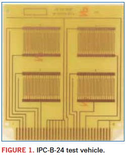
From an electronics industry perspective, one of the primary work horses for materials qualifications since the early 1990s has been the IPC-B-24 test vehicle (Figure 1). IPC-B-24, along with most other IPC test vehicles, was designed primarily as a material qualification vehicle.3 When companies like IBM queried contract manufacturers (CMs) or paste/flux manufacturers concerning SIR, most often the data provided came from the B-24 TV per the IPC test method.5 The IPC-B-24 test vehicle was originally designed to be an inexpensive vehicle for examining the relationship between laminate, metallization, and flux in wave soldering applications and is the standard test vehicle for flux qualification to J-STD-004.3,7 Though designed for wave soldering, its use was expanded to evaluate SMT pastes and fluxes, including the mixing of materials. It has four SIR combs with 16 mil lines and 20 mil spaces that were chosen to permit wave soldering without bridging. The PCB material is FR-4 with copper traces. There are no through holes, internal planes, or components.
As an initial, low cost and simple test vehicle to evaluate materials, including the mixing of fluxes, IPC-B-24 is adequate, as demonstrated by its widespread usage. To propose that the SIR data from this PCB can be bridged to actual products is much more difficult to conclude. It is also clearly not a good test vehicle to qualify a new EMS as having acceptable assembly practices. Therefore, even though this test vehicle became the industry standard, several OEMs required additional testing of a more product-representative test vehicle.
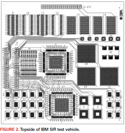
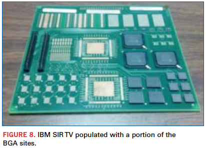
As product cycle times shortened and cost challenges grew, it became more difficult to design and procure product-specific SIR test vehicles. Therefore, IBM took the initiative to design a generic, product-like test vehicle. In late 2002, IBM released a double-sided SMT test vehicle designed to evaluate the technology ground rules and most complex components used in IBM products at the time of its release. Figures 2 and 3 show the top- and bottom-side layouts of this assembly. Some of the key technologies and design features are as follows:
- Card size – 152mm x 152mm (6" x 6")
- Board includes internal power planes
- 8 – Type 2, 64 pin, 0.8mm pitch TSOPs
- 8 – 9x7, 153 pin, PBGA SRAM packages, 1.27mm pitch; 4 on front and 4 directly opposite on back with shared via
- 1 – 208 pin, PQFP, 0.5mm pitch with a comb pattern underneath the component to evaluate flux entrapment (similar to IPC-B-52)
- 1 – 256 pin, PQFP, 0.4mm pitch with a comb pattern underneath the component to evaluate flux entrapment (similar to IPC-B-52)
- 6 – 75 pin, CSP packages, 0.5mm pitch
- 4 – 22x22, 484 pins, 1mm pitch BGAs, two of which are back-to-back
- 6 – 13x13, 144 pin, center depopulated, 0.8mm pitch; 2 on front and 2 on back with shared via
- 6 – 24 pin, 0.5mm pitch QFN
- 50 – 0402 capacitors with bare trace (i.e., no solder mask) running under the components
- 37 – 0603 capacitors with bare trace running under the components
- 16 – 0805 capacitors with bare trace running under the components
- 27 – 6x8, 48 pin, BGA, 0.75mm pitch; 6 on top and 6 on bottom with shared via.
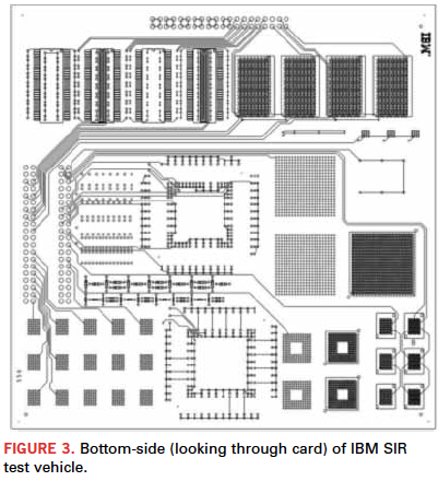
Full SIR testability is possible with or without components present. This test vehicle, which also includes the capability to measure solder joint continuity, is used by EMS firms to evaluate the mix of chemistries and their assembly processes. It is still in use today, although updates are needed, including the addition of wave-soldered risk sites.
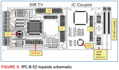
SIR TVs. IPC is in the process of attempting to establish an industry standard SIR test vehicle. Its proposal is the IPC-B-52 card, donated to IPC by Rockwell Collins (Appendix A). The genesis of this design is attributed to the National Physical Laboratory (NPL) and Gen3. A research paper on IPC-B-52 stated, “The goal of this search effort was to develop a test vehicle, building upon successes and lessons learned from past test vehicles, which would represent mainstream electronics manufacturing, at a reasonable price, usable by many.”2
The IPC-B-52 design includes four separate areas / test vehicles:
- SIR test vehicle.
- Ion chromatography coupon.
- Solder mask adhesion coupons (quantity = 2).
- SIR mini-coupons (quantity = 2) – primarily for evaluating raw board PCB cleanliness at the PCB supplier versus incoming to the PCB assembler.
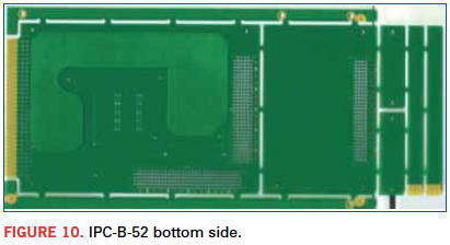
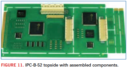
The test vehicle has no internal power planes. Components are on the bottom and topside of the PCB, so like most product boards today, the test vehicle experiences two-pass oven reflow, but the backside is minimally populated with only 20 0805 components grouped together. It also has plated-through holes and wave-soldered connectors with SIR patterns. A key improvement over IPC-B-24 is that IPC-B-52 is designed to have components assembled, which is much more representative of real product. This creates entrapment sites for deleterious process materials, such as flux. Other features include:
- The ability to perform SIR testing without components. Testing without components emulates the material qualification purpose of the IPC-B-24 TV.
- The test vehicle can be ordered from the same PCB supplier used for product, so laminate materials, metallization, solder mask, etc. can match existing production design points. This is made possible by IPC making the board design data available to users.
A more detailed description of IPC-B-52 can be found in the literature.1,2,8,9
IPC-B-52 lessons learned. As industry migrated to Pb-free chemistries, the learning curve to identify acceptable material solutions has been quite steep. Companies like IBM have EMS partners located all over the world. To sufficiently manage the variety of assembly chemistries found across these global suppliers, IPC-B-52 has become attractive as a means to compare material sets of EMS that have chosen various material suppliers or formulations. This is especially true and cost-effective when an EMS has already collected SIR data on this test vehicle as part of its own material selection qualification.
In the past year, IBM worked with a contract manufacturer to evaluate water-soluble, Pb-free flux chemistries (solder pastes, wave solder fluxes, rework tacky fluxes and liquid repair fluxes).10 As part of this qualification effort, IBM utilized the IPC-B-52 TV to evaluate and compare top chemistry candidates. Test vehicle assembly was performed at IBM in Poughkeepsie, NY. From this and previous EMS build experiences, the team identified a list of lessons learned for assembling the IPC-B-52 test vehicle. This information was provided to the IPC’s Surface Insulation Resistance Task Group (5-32b), which began evaluating the submission at IPC Apex 2012.
Lessons learned and the feedback from the IPC TG are shown in Table 1. Recommendations for improvements to the IPC-B-52 TV, along with feedback from Apex 2012, are in Appendix A.
[Ed.: To enlarge the figure, right-click on it, then click View Image, then left-click on the figure.]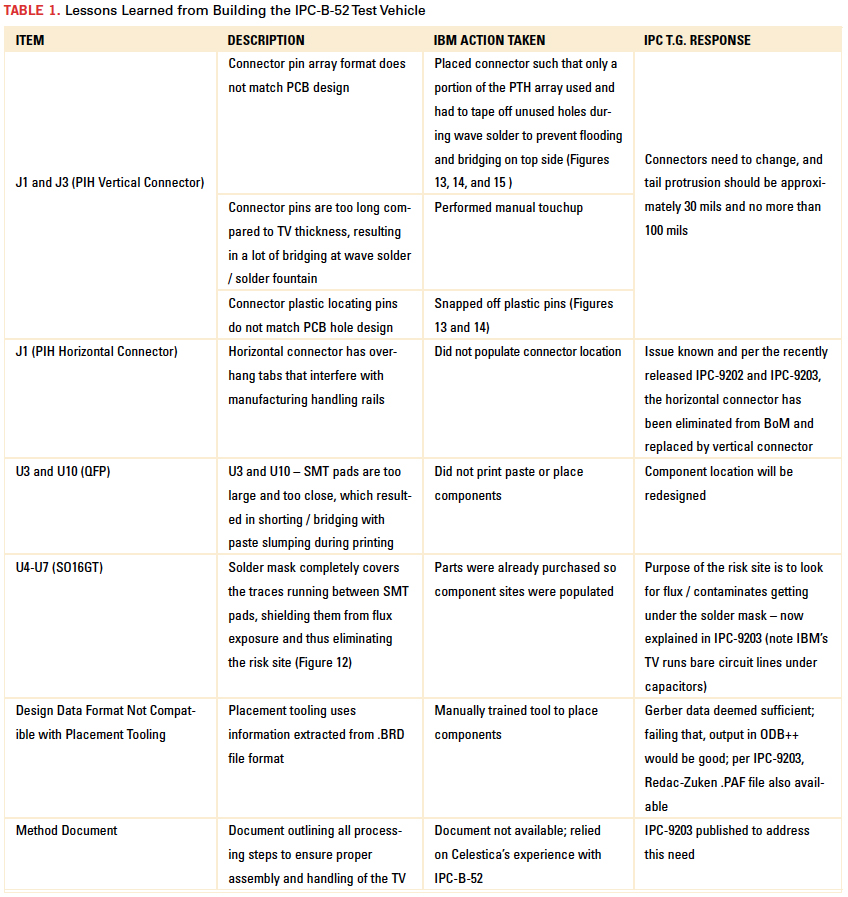
SIR TVs: Looking ahead. IPC-9202 discusses “process characterizations” and “process qualifications.” It defines a process characterization as a comparative examination of the interaction of materials and process parameters. A process qualification is defined as the generation of “objective evidence” for purposes of demonstrating materials and process compatibility for an assembly standard (e.g., J-STD-001). In terms of SIR, it states a process qualification should demonstrate that a proposed manufacturing process or process change can produce hardware with acceptable end-item performance related to cleanliness. It emphasizes that for process qualifications the test vehicle materials and processing must be representative of product. IPC-9203 states that the IPC-B-52 test vehicle can be used to evaluate and optimize a manufacturing process, or to provide objective evidence that a chosen manufacturing material set and manufacturing process are compatible from a cleanliness standpoint. Last, IPC-9202 states that the user is responsible for assessing whether components and other design characteristics of the IPC-B-52 test board are sufficiently representative of their production design(s). This is the ultimate test in assessing whether the IPC-B-52 test vehicle has achieved its goal of “being representative of mainstream electronics and useable by many.”2
As most IPC test vehicles consisted of boards without components, IPC-B-52 is a significant improvement. The presence of low-standoff components provides material entrapment areas that make the evaluation of SIR more product-like. Yet, when IPC-B-52 is compared to real product, it may lack many key features the user might desire in order to conclude it a good representation of their assemblies. These differences are likely to be less critical when performing new material or a mix of material qualifications. In the case when the user desires a process qualification, focus items are generally items such as:
- Qualification of a new CM for which the user has limited knowledge of its capabilities.
- Qualification of a CM for which the user is familiar, but now that CM is asked to build a higher complexity assembly.
- Verification of the adequacy of water wash tools, fixtures, wash parameters, etc. to remove water-soluble flux residues.
- Verification that thermal profile oven parameters are sufficient to fully activate fluxes.
- Assessment of the rework process, including:
- Verification that the site dress process and solder paste or flux application does not result in excessive material being applied (excessive flux entrapment).
- Confirmation that the hot gas rework tool sufficiently activates the flux.
Test vehicle versus product differences may mean the difference for reliable product. In comparing IPC-B-52 or any test vehicle to actual product, there are design elements that the user might want to consider incorporating.
PCB considerations. Nearly all PCBs have a multilayer stack-up, with multiple ground/power planes and signal planes. Components are wired to these layers via plated through holes. When reflowing the solder to attach components to the PCB, these connections absorb heat, making achievement of the desired thermal profile more difficult. The plated through holes also provide flux entrapment areas, especially as a result of component rework. Although it is true that an SIR TV’s primary purpose is to evaluate surface cleanliness, the actual resultant surface condition of the user’s test vehicle may not be representative of their actual product if these features are not present.
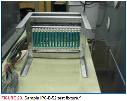
The IPC-B-52 test vehicle utilizes a card edge tab (Appendix B), rather than a through hole connector to interface with the SIR testing setup (Figure 20). This has its advantages for ease of testing, but limits the coupon thickness to the range the mating connector was designed to accept. Therefore, if the user were to desire to use a TV stackup and thickness representative of their product, the entire test fixture would have to be modified to use connectors that accepted the greater card thickness. If the IPC-B-52 test vehicle designed with a PTH or compliant pin connector can be ordered in variable pin lengths, then the SIR test setup would not have to be modified to account for the varying test vehicle thicknesses. Also, if IPC-B-52 were to change to this new connector concept, it would also be possible to design a reusable adapter card such that existing IPC-B-52 SIR test setups could still be utilized.
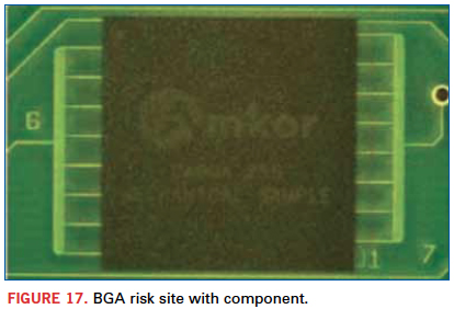
BGA considerations. IPC-B-52 contains one 16x16, 1mm pitch, 256 I/O BGA device (Figure 17). Per IPC-9203, many users have asked why the test vehicle was not designed with a larger, more challenging BGA component, such as one with 1700 solder connections. The response is that the 256 I/O BGA was chosen because it is available as a true mechanical dummy. A mechanical dummy is required because alternating rows of solder balls are biased against one another, and if the module were functional, this would make testing impossible by this method. IPC-9203 suggests that if the user wants to incorporate a larger BGA device to make it more representative of their product, open space is available to do so.
A workaround for the requirement to find large, dummy BGA devices is to use a different wiring scheme, per Figure 4. (Note: The full wiring scheme is not shown, but rather just the upper left corner.) A common method for connecting a BGA solder ball to a PCB is through a dog bone connection. An example of a dog bone is shown on the left side of Figure 4. A dog bone is made up of a solder pad for the solder ball, a plated-through hole to connect that pad to internal PCB wiring, and a small circuit line connecting the two. When wiring the test vehicle, the connection between the copper pad and the PTH can be left out of the artwork. The PTHs can be stitched together to form one part of the SIR comb and the solder pads stitched together to form the other part of the SIR comb. By using this wiring scheme, the user is no longer limited to the use of a dummy component. A wired functional component will not impact the SIR testing. This provides the following advantages:
- Scrap components can be utilized, so the user can assemble modules from their actual product to the test vehicle.
- The BGA location can be made to accommodate a very large BGA array, but BGAs with a smaller array will work on the same location.
- The PTHs provide flux entrapment areas.
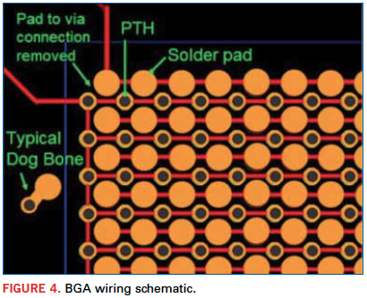
Figure 4 does not show the SIR combs extending beyond the outline of the module body outline, shown in dark blue, but this is recommended if possible, to allow
easier failure isolation. This concept is utilized by IPC-B-52 and shown in Figure 17.
A disadvantage to the alternate wiring scheme shown in Figure 4 is that it alters the thermal characteristics versus product, as the thermal paths between solder balls and the internal layers of the card have now been separated. Despite this, with the PTHs present and a multilayer PCB, the design will be more thermally representative of actual product than one like IPC-B-52. There is also an increased risk for pad delamination using this proposed wiring design when a rework evaluation is done on the BGA module.
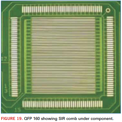
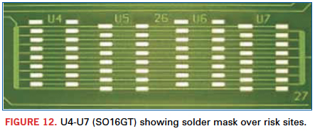
Rework considerations. Rework operations can create surface cleanliness concerns, and it is therefore advisable to ensure that any TV have risk sites representative of the highest difficulty rework sites on the user’s product. For water-soluble fluxes, the user may even want to create worst-case scenarios by purposely putting excessive flux under components to assess the water wash tools and process parameters. The SIR combs, under the two QFP locations and one BGA location on IPC-B-52, can be used toward this purpose (Figure 19). The user can have the components removed by the rework process and coated with, for example, a liquid tack flux. After replacing the components with the rework process and sending the assembly through wash, the effectiveness of the cleaning process could be assessed through the SIR testing. If no-clean flux is used, the user may still want to create a worst-case scenario by the same means to determine if the thermal exposure is adequate to fully activate any excessive flux that might be present.
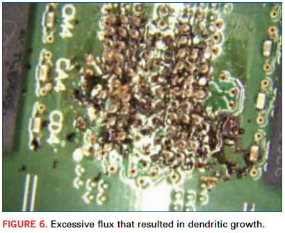
For double-sided product, especially with mirrored components, with shared PTHs, it is advisable to include this configuration in the SIR TV. (IBM’s SIR TV has 10 BGA-mirrored BGA risk sites with shared via; see Figures 2 and 3.) The presence of unactivated flux for the mirrored BGA rework operation has been observed in the past.4 Figure 5 illustrates the process that resulted in the excessive, activated flux, and Figure 6 shows the PCB with the mirrored BGA removed.
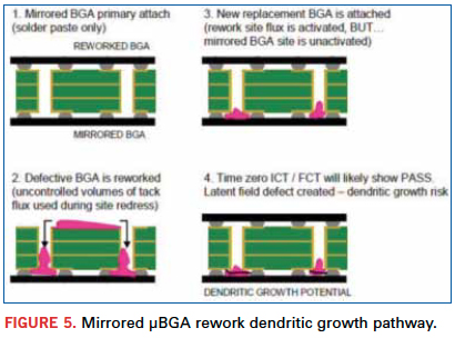
The components were initially attached with solder paste without the use of additional flux. The top component was found to be defective and needed replacement. The component was removed and liquid tack flux used during site dress. The flux amount was found to be excessive such that the flux flowed through the PTHs and collected between the bottom of the PCB and the mirrored component. The rework thermal profile was complicated by the presence of neighboring temperature-sensitive components that limited the rework peak temperature. As a result, unactivated flux was present between the bottom side component and PCB.
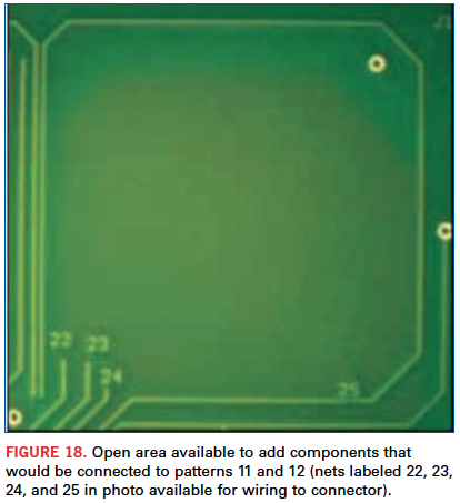
Increasing IPC-B-52 risk sites. Many users of IPC-B-52 have specifically designed test fixtures and setups. It is therefore desirable for those users to continue to use the same IPC-B-52 configuration. The question is how to add these additional, more product-like elements to a test vehicle with limited I/O. As shown in Figure 18, there are only two more open test patterns available for testing using the card edge connector. Additional test patterns can be added by grouping test patterns. For example, if the addition of mirrored components were desired, a SIR comb on the top could be mirrored with one on the bottom (Figure 7).
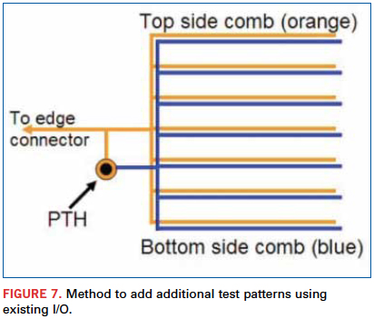
The existing circuit line to the topside comb could be branched to a PTH that connects to a comb on the bottom side of the card. Should an SIR failure occur, it would not be possible to determine the fail location (i.e., top component or bottom component) by looking at the test readout alone. The part would need to be removed from the stress chamber (at end of test), and the circuit line connecting the top and bottom combs would need to be cut to determine which had failed.
Conclusions
It is clear based on the release of IPC-9202 and IPC-9203 that the SIR Task Group is actively working to improve the IPC-B-52 test vehicle and standardize its use to meet industry needs. Adoption of a test vehicle that contains surface mounted and wave soldered components is a significant improvement over the historical family of IPC test vehicles, including the IPC-B-24 design. It is also acknowledged that SIR Task Group is planning to release an updated IPC-B-52 design to address some of the current design and manufacturing deficiencies. Companies like IBM are continually looking for more efficient and cost-effective approaches to perform qualifications. Adoption of an industry standard SIR test vehicle and test methodology is therefore very attractive. For materials qualifications, IBM and other companies have utilized the IPC-B-52 test vehicle and will continue to do so.
As companies leverage new CMs in low-cost geographies, there will be a need to verify assembly and rework processes to ensure product reliability. In cases in which IPC-B-52 is deemed not adequately product-like, the user will need the flexibility to easily modify IPC-B-52 to make it so, or will need an alternate test vehicle design such as the IBM SIR TV. It is hoped that some of the design options proposed here will be considered by the IPC SIR Task Group as a means to provide users the flexibility to make the IPC-B-52 more product-like.
References
1. IPC-9201A, “Surface Insulation Resistance Handbook,” August 2007.
2. D. Pauls and C. Slach, “Process Qualification Using the IPC-B-52 Standard Test Assembly,” IPC Printed Circuits Expo and Apex Proceedings, February 2006.
3. IPC-5702, “Guidelines for OEMs in Determining Acceptable Levels of Cleanliness of Unpopulated Printed Boards,” June 2007.
4. M. Kelly, M. Ferrill, P. Snugovsky, R. Trivedi, G. Dinca, C. Achong and S. Bagheri, “Rework Process Window and Microstructural Analysis For Lead-Free Mirrored BGA Design Points,” IPC Apex Expo. Proceedings, March 2009.
5. IPC-TM-650, Test Methods Manual, Section 2.6.3.3, “Surface Insulation Resistance, Fluxes,” June 2004.
6. IPC-TM-650, Test Methods Manual, Section 2.6.3.7, “Surface Insulation Resistance,” March 2007.
7. IPC J-STD-004B, “Requirements for Soldering Fluxes,” November 2011.
8. IPC-9202, “Material and Process Characterization/Qualification Test Protocol for Assessing Electrochemical Performance,” October 2011.
9. IPC-9203, “Users Guide to IPC-9202 and the IPC-B-52 Standard Test Vehicle,” May 2012.
10. M. Kelly, M. Ferrill, W. Ma, N. Ranadive, C. Ndiaye, S. Bagheri, and P. Kapadia, “Water Soluble Lead-Free Process Chemistry For High Voltage and High Reliability Hardware Requirements,” SMTAI Proceedings, October 2012.
Ed: This article was first published in the SMTA International Proceedings, October 2012, and is published here with permission of the authors.
Mitchell Ferrill is card assembly qualification engineer; Matt Kelly is senior technical staff member; Wai Ma is senior engineer; Nandu Ranadive is development engineer; Cheikhou Ndiaye is technical program manager, and Jim Bielick is an engineer at IBM; ferrill@us.ibm.com. Simin Bagheri is a corporate process development engineering consultant at Celestica; sbagheri@celestica.com.
APPENDIX A
IBM / Celestica provided the following recommendations for improvements, and the SIR Task Group has taken the following actions to date:
- Add depanelization scoring
a. Purposes:
i. Make separating the coupons easier and manufacturing rails easier.
ii. Avoid risk of debris / contamination from mechanical routing
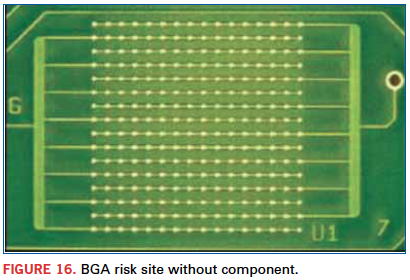
b. IPC Action: Considering solutions, but no clear consensus to date; the PCB is available with and without manufacturing rails, but if the manufacturing rails, users would prefer to have more space between the through hole connectors and the edge of the card - Create classical “dog bone” structures with PTHs in the BGA site to make TV more product-like (current design has only unconnected Cu lands – see Figure 16)
a. Purposes:
i. Create realistic thermal paths requiring more heat to be applied to achieve reflow
ii. Provide better mechanical anchoring to minimize pad delamination during rework (module removal and site dress)
b. IPC Action: Most of task group felt they were not needed, especially if the pads are solder mask defined - Add internal power / ground layers
a. Purpose – make TV more product-like / realistic by providing heatsinking, especially for rework
b. IPC Action: Recommendation rejected
i. Not needed – purpose of TV is to test surface cleanliness
ii. Would raise cost significantly
iii. Interferes with backlight examination of bare boards
iv. Considering adding internal Cu in form of checkerboard pattern with openings - Add additional component footprints
a. Purpose: To keep pace with today’s board designs (FC-QFNs, RNETs, 0201s, etc.)
b. IPC Action:
i. Task Group received many different proposals on components to add
ii. Propose creating library of SIR patterns – these could be used for companies to create their own SIR TVs or placed in the open areas on the current B-52 (see Figure 18 or IPC-9203)
Best-in-class testers combine multiple AOI, text verification and impedance testing in one machine.
Assembling a single PCB and thoroughly inspecting it before turning on a production line – also known as first-article inspection (FAI) – is critical to a successful PCB assembly process. It ensures the right components are in the right places, and that the assembly meets its manufacturing specification. FAI is important at all stages of a product’s life. In the prototype stage, it delivers correct assemblies so designers can debug the circuits instead of the manufacturing process; in production, it verifies the correctness of the first product before building hundreds, or even thousands, of them.
Failure to capture mistakes in circuit assembly methods, equipment setups or programs can result in delayed development progress, lost production, risky rework or even product recalls – all of which cost unbudgeted time and money.
Typical defect modes found in PCB first article inspections include wrong component values or sizes, misplaced components, reversed polarity or missing components.
Counterfeit components that slipped past incoming inspection may also be identified at FAI.
Different PCB assemblers employ different FAI techniques. Checks for component presence, polarity, placement or size are performed by operations that range from manually comparing the PCB with a drawing to semiautomated or fully automated optical inspection (Table 1). Current methods of first article inspection on a PCB assembly are mainly optical. (Ironic, isn’t it, considering that the product being tested is electronic?) Optical inspection is only a partial answer at best. Electrical verification is also required, especially on high-reliability products. Many companies now specify electrical verification as part of their FAI requirement, especially those employing the AS-9000 Quality System (sidebar).
[Ed.: To enlarge the figure, right-click on it, then click View Image, then left-click on the figure.]

Electrical verification of the values of unmarked components may be done manually with a meter and a BoM checklist, or by in-circuit testing, if available. On prototype runs, ICT is often not available, so verification is performed manually. This can take hours, keeps the assembly line down, and is prone to human error and fatigue. Some assemblers do not test the electrical integrity of the PCB assembly in the prototype stages because of the time requirement. Electrical verification should not be optional when manufacturing electronics assemblies, as component values are critical to the product’s functionality.
A new genre of FAI testing equipment is emerging to support the need for more efficient, effective inspection. These machines typically employ semiautomatic optical inspection methods, which improve inspection speed and accuracy and ease operator fatigue. They are easy to program with BoM and Gerber files, and are intuitive for operators to use. Their cost and portability between assembly lines enhances their ROI, and their ability to prevent costly mistakes makes them highly desirable for prototype or batch-style assembly operations.
FAI inspection systems vary greatly in feature content and user benefits. The most basic machines scan images of the PCB assemblies and display programmed areas of the scanned images for operator inspection. More advanced systems offer higher resolution cameras on X-Y gantries to allow operators to pan, zoom or change lighting in real time to better see the objects under inspection. The most sophisticated systems integrate automated and semi-automated optical inspection with electrical testing to provide the most comprehensive first article verification.
The fully integrated machines utilize key aspects of AOI, electrical test and semiautomatic inspection as they apply specifically to FAI:
- The AOI function inspects for component X/Y location, rotation, and size.
- An Optical Character Verification (OCV) function inspects the text or other markings on the component.
- An LCR meter measures the impedance of chip capacitors and resistors (Figure 1) to verify the values listed on the BoM. Value checking on parts smaller than 0402s is critical because the components are too small to bear identifying text and cannot be verified optically.

If automated checks identify any discrepancies throughout the optical or electrical test sequences, the machine uses a semiautomatic mode to step nonconforming components under the camera for positive verification. Figure 2 shows the high-magnification camera view of the component test probes.
[Ed.: To enlarge the figure, right-click on it, then click View Image, then left-click on the figure.]
After the first article has been verified, the data can be stored and uploaded to various data management programs and quality assurance reports. These systems can replace nearly all paper-based FAI documentation like diagrams, checklists or other recording media. The operation speed and automatic report generation can reduce the time needed to perform an FAI and improve the accuracy of the entire process.
Summary
FAI testers validate PCB assemblies by various methods. Best-in-class FAI testers combine multiple methods into one machine: AOI, text verification and electrical impedance testing. They also eliminate the paperwork of inspection documentation and report generation.
Simplifying, automating and documenting the PCB FAI process according to international standards, while incorporating both optical and electrical tests, will contribute to improved product reliability and lower manufacturing costs.
References
1. Goodrich ISR Systems, First Article Training Ref AS9102, Rev A.
2. Robert Morris, “Enhance First Article Inspection,” Quality Magazine, July 16, 2007.
Matthew Holzmann is president of CGI Americas (cgi-americas.com); matt@cgi-americas.com. Chrys Shea is founder of Shea Engineering (sheaengineering.com); chrys@sheaengineering.com.
Who pays for those failures in the corner that are going nowhere?
It is a disconcerting and time-consuming fact of life in our industry that the level of bluff and bluster on the part of OEM supply chain personnel often is inversely proportional to their technical grasp of the subject matter.
This leads to pearls of wisdom like these:
- “I don’t care how you do it. I just want good boards.” A common refrain. Those of us graced with the task of sitting on the seller’s side of the desk have all heard it. The more astute among us also have picked up the subtext: “And I don’t want to pay for testing.”
- Poof. It’s black magic, of the free variety. Just manage a flawless assembly process, and all will be well, notably without testing.
- Yeah, right.
- Your customer probably wants motherhood, apple pie, clean air and water, two cars in every garage, and a chicken in every pot, while we’re at it. All for free as well. Kind of like school bond issues: We don’t pay for them, do we? Somebody else does? Out of sight, …
- Nonetheless, that’s your problem, esteemed Contract Manufacturer. A cost of doing business, but certainly not one to be passed along. So stop whining and suck it up, especially if you want future business.
- The customer has spoken. And as we know, he/she is always right. Case closed.
Now what? Panic at the thought of that test expense burning a hole in your pocket? Give it all up? Clearly we are all going to die! (Just kidding. I’m writing this on April 1.)
Seriously, it’s time for an adult conversation with your customer about testing. It is a legitimate cost of assembling a printed circuit board. As legitimate as solder paste, stencils, reflow ovens, chip shooters, payroll and advertising. And somebody must pay those costs.
Why is testing necessary? Because stuff happens. And somebody must catch it. Or else hordes with clipboards materialize at the back door, wanting to know why and how and where about everything. In quintuplicate. Suddenly, Somebody is justifying rather than manufacturing. And Somebody is undisputedly not a charity.
It doesn’t take a Six-Sigma Black Belt with a minor in Lean manufacturing to recognize that machines break, work instructions are misinterpreted, chemicals fail to live up to their shelf lives and humans screw up. In short, stuff happens.
Still not convinced? Want to see some true believers? I bet they’re testing 787 lithium batteries right now at Boeing like their lives depend on it. And in a way, they do.
Now I have your attention.
But do I have your concern, and, most important, your buy-in? Still rationalizing that your process is robust enough to avoid testing? Still insist that it’s best not to raise neuralgic issues like testing with the customer?
Remember the iron law of the Power of One. As in 1000 attaboys cannot erase the fallout from one Oh…(you know what).
As they say, you can pay me now or pay me later. I can help you now, or I can attempt to salvage your reputation later. A cliché, yes, but occasionally clichés are true. And painful. Noticeably the part called “later.” “Later” is usually associated with hard, negative numbers.
So consider this an intervention. An appeal to face facts and admit what common sense dictates. It’s for your own good, trust me. I know these things. I once was in your shoes.
Testing cannot, and should not, be avoided.
There. With that as our premise, it’s time to talk seriously about broadening horizons and removing past perceptions.
The good news is that nowadays you have many cost-effective options. Your choices are not constrained by ICT – and its reputation for cost-prohibitiveness – alone. We have flying probe and JTAG/boundary scan. We even have flying probe incorporating JTAG/boundary scan. We have varieties of x-ray inspection: 2D, 3D, AXI and even variations on CT scanning, and we can do all of it fast and a lot cheaper than you may think at first glance.
I know what your next objection is going to be: We already have functional testing, and it’s good enough.
Really?
What do you do when boards fail? Who pays for those failures? What do you do when your functional test apparatus – most likely designed to suit a laboratory or an NPI environment – fails under the demands of production. Also, how effective is your functional test setup at fault diagnostics? Do you get anything more substantive than a red light or a green light? Again, who is paying for those failures piling up in the corner and going nowhere? Did you account for this attrition in your original quote?
Uh oh. Forgot something?
Wouldn’t it be preferable to have a test regime in place that directly contributes to higher functional test yields? And if it could be demonstrated that implementation of such a regime generates a payback for the incremental cost of testing?
Still think your process is perfect and you don’t need testing?
We’ve barely touched on the environmental considerations. Remember those boards piling up in the corner? Besides adding to your “conversation starter” repertoire, what are they doing for you? Nothing good, that’s for sure. But wait, there’s a solution for those problems too. Testing enables you to rehabilitate and even recycle many of those “bad” boards and return them to productive service, thereby restoring some lost revenue, while contributing to a greener world. How? Because resources aren’t needed to make fresh boards from scratch. Less e-waste means fewer landfills, with more metals and other materials in use rather than in the ground. It’s economical and environmentally friendly. Statisticians (and CFOs) call that a win-win. And you thought all we Test Guys do is probe for opens and shorts.
Green virtue aside, it’s still cost-prohibitive, you insist. Oh yeah? Ever heard of something known as the Cost of Quality?
It’s that pesky concept in which quality costs are a prime factor in quantifying the total cost of manufacturing, including part defects, process deficiencies, and time. Lots of time. Like high-paid engineers’ time, trying to figure out what went wrong, and how to fix it. Time diverted from shipping fresh product and developing new products until the crisis has been addressed and abated. And management time, fighting fires and spinning perceptions. Stated somewhat differently, the Cost of Quality isn’t the price of creating a quality product or service; it’s the cost of not creating a quality product or service. That cost finds no clearer expression than in the unplanned, unnecessary expenditure of peoples’ time.
It’s unnecessary. There is a solution. Trust me.
Just saying…
Robert Boguski is president of Datest Corp., (datest.com); rboguski@datest.com.
The road less traveled is often the fastest.
Sometimes a circuit board can be populated much quicker than a machine can solder it. If you find that boards are piling up waiting for the machine to finish, there are a number of different ways to reduce the throughput time. I will address one of them this month.
When drawing a path for the machine to follow, begin your next path close to where your previous path stopped. A machine that travels a long distance, crisscrossing back and forth around the board, will dramatically increase cycle time and decrease efficiency.
I know this sounds obvious, but by being diligent with this practice, we have decreased cycle times by as much as 50%. How? When you first program the board, you may not have considered every little detail. Once a couple of boards have been run for the first time, issues begin to appear, such as a missing part or the nozzle making contact with a bottom-side surface mount part. The natural response is to go into the program and add a couple of new paths. But each occurrence adds complexity, and if you’re adding complexity without considering where your machine needs to travel, the result will be a lot of time wasted with the nozzle traveling all around the board.
Chris Denney is chief technology officer at Worthington Assembly (worthingtonassembly.com); cdenney@worthingtonassembly.com.
http://circuitsassembly.com/cms/images/stories/ArticleImages/1305/soldering.jpg
EMS companies showed their flexibility in 2012, adjusting to slowing consumer and defense markets.
2012 was a reminder of the somewhat fragile nature of the customer-manufacturer outsourcing relationship.
A pair of Top Tier EMS companies absorbed potentially staggering blows from the losses of their largest customers in 2012, a year in which a heretofore fast-growing mid-tier EMS also saw its largest customer shrink.
To recap, in June, RIM announced it would cut ties with Celestica. (RIM also dumped Flextronics.) Then in the third quarter, Juniper let it be known it would depart from Plexus. This was an even bigger surprise, as Juniper not only made up 16% of Plexus’ sales, but had been the EMS firm’s largest customer since 2003.
Also, General Dynamics trimmed its relationship with No. 43 OnCore, and No. 29 Fabrinet’s largest customer, Oclara, terminated their relationship, although that move was seen as a negotiating ploy.
Elcoteq, RIP. To see what the loss of a leading customer can do, we need look no further than Elcoteq. With the loss of Nokia, the once-massive Elcoteq business evaporated, although to where, no one seems entirely sure. One likely suspect: Eolane. While as of March last year, the bankrupted Elcoteq had shuttered a total of seven operations in Shenzhen, Switzerland, Finland, Luxembourg and Mexico, Eolane, the French EMS, was busy acquiring its sites in Estonia and India. It’s a sad demise for Elcoteq, which ranked sixth in revenues among EMS companies as recently as 2008.
Meanwhile, No. 35 Eolane has emerged as France’s second-largest EMS, behind No. 21 AsteelFlash. (France did not have an entry on our original list, which covered calendar 2008.) Both firms are looking at additional growth through acquisitions, with AsteelFlash having gobbled up former Top 50 entrant ElectronicNetwork in August.
2012 was a tough year for most EMS companies. Outside of M&A activity, it’s tough to grow when the end-markets are sliding.
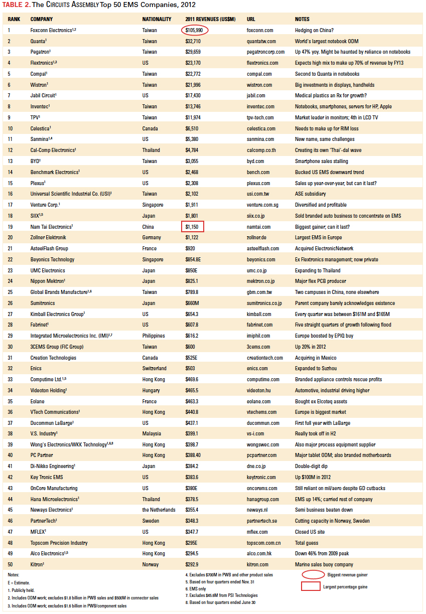
At least a dozen companies declined year-over-year, with Flextronics leading the way thanks to its changing business model, which saw it exit the low-margin PC ODM business. Celestica and SIIX were among the largest revenue decliners, but SRI Radio Systems arguably had the worst year, declaring insolvency before being snapped up by TQ-Group of Germany.
A record 20 companies topped the $1 billion mark, although that comes with the disclaimer that this year we began including the ODMs (see below). Foxconn grew the most, up nearly $13 billion (slightly more than the size of Celestica and Sanmina combined). The newest entrant, No. 19 Nam Tai, was also the biggest gainer, up a startling 91% (not a typo) from 2011. Mergers and acquisitions notwithstanding, other big winners included No. 25 GBM, No. 30 3CEMS, No. 33 Computime and No. 42 Key Tronic.
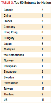
The ODM effect. Hardcore Circuits Assembly Top 50 watchers might ask, “Where did all these Taiwanese companies come from?” The answer is they were always around, just not included. The reason: ODMs have for various reasons traditionally been excluded from EMS company lists.
Lately, we’ve found the rationale for separating the two groups weak. ODMs generally compete with EMS companies for business in certain large sectors (computing, networking, consumer), and several so-called EMS companies (Foxconn, Flextronics, 3CEMS, Sanmina, to name a few) have for years operated what analysts refer to as ODM businesses. No list we know of has discounted the ODM sales from EMS revenue, however. Instead, they seem to dismiss most of the Taiwan ODMs, yet include their Western counterparts. By definition, an ODM designs and manufactures a product to be branded by another firm. Every electronics end-product that’s sold is branded in one way or another. And ODMs today are chasing margins as much as markets, meaning they are coming in closer competition with the “pure” EMS firms. We find the distinction between EMS and ODM too fine to be relevant today, thus the presence of several “new” listings.
To muddy the waters further, not every company that is called an ODM meets that definition. Two big Acer spinoffs, Qisda and BenQ, sell primarily their own branded goods. Thus, they aren’t listed here. On the other hand, Wistron, another Acer spinoff, makes the list because the IT, computer and consumer electronics it designs and builds are on behalf of OEM customers, as does TPV, despite a joint venture last spring that left it owning 70% of Philips’ TV division.
Insofar as successes in 2012 went, Nam Tai’s surge was the story of the year. The China-based company finally saw its investments in LCD modules for smartphones and tablets pay off, and was aided by sales of LCDs to the automotive industry, particularly US OEMs.
Can it last? Nam Tai has invested heavily in capacity in southern China, and has another 1.2 million sq. ft. “parcel” of land that it plans to develop – twice the size of its present Shenzhen campus. This is all the more amazing because Nam Tai says its two existing factories are capable of about $150 million in revenue per month each, which suggests its current capacity utilization is around 30%.
Hits and misses. We overstated OnCore’s revenue last year. We pegged it at $640 million on the basis of incorrect information that Victron, which it acquired, had much higher sales than it did. The correct revenue was $420 million, per the company. And the rule of thumb for flex PCB producers is that 40% of their revenue comes from assembly. Unfortunately, we miscalculated for Nippon Mektron last year and inadvertently gave it credit for 60%. Finally, apologies to 3CEMS, which we listed as a Chinese company, when in fact it is Taiwan-based.
All company revenues reported here are converted to US dollars (Table 1), and to the extent possible, we use calendar 2012, regardless of any individual company’s specific fiscal year. Because of differences in fiscal years and constantly fluctuating currency rates, company-reported revenues might vary somewhat from what is shown here. As always, any errors are our own.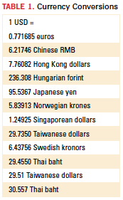
For those who are wondering which EMS companies might have made the cut had we continued the practice of ignoring most of the major ODMs, that partial list would include (alphabetically) CTS, Scanfil, Selcom, SVI Public Co. and TQ-Group.
[Ed.: To enlarge the figure, right-click on it, then click View Image, then left-click on the figure.]
Mike Buetow is editor in chief of PCD&F and Circuits Assembly; mbuetow@upmediagroup.com.
Ed: For the 2011 Top 50, click here.
For the 2010 Top 50, click here.
For the 2009 Top 50, click here.

Press Releases
- Metal Etch Services Installs First NEVIS Stencil Laser System in the US
- RBB Welcomes Shawn Myers as Engineering Project Manager
- ECIA’s Market Sentiment Index Average Hits Five-Year High in June Industry Pulse Survey
- Incap Slovakia invests in cleanroom capability to support semiconductor manufacturing requirements