

Openair-Plasma as a pre-treatment for bonding and sealing in electronics applications
The requirements for electronic assemblies are becoming more and more demanding. This is not only due to an increase in packaging density and progressive miniaturization, but also to an increase in areas of application. For example, reliable bonding and sealing processes are becoming more important in electronics manufacturing, due to electric vehicles and the associated integration of touch displays, highly sophisticated security and sensor systems or the increased installation of cameras. Therefore, plasma as a pre-treatment for bonding and sealing is moving into the focus of developers, production specialists and quality managers.
"We see an increasing number of bonding and sealing applications in the electronics industry", says Nico Coenen, Business Development Manager Electronics Market of Plasmatreat GmbH, assessing the developments in his sector. With regard to the subject of sealing, the focus of the EMS companies is to protect the electronics for the harsh environment. For an effective housing made from aluminum or plastic, the seal must be hermetically closed so that no moisture can get into the box. The pretreatment with Openair-Plasma is crucial for a stable connection between casing.
The situation is similar in display and HMI production. "In the process of manufacturing such products, the interior must be reliably protected from dirt or other environmental influences. However, since metal and plastic are often combined in the casings, we are being confronted with a particular challenge here, since these materials are very complex to bond and thus seal," explains Coenen. In this case, Openair-Plasma technology is used in the final assembly to bond the different materials such as metal, glass and plastic in a stable manner. A clean and stable bond between these materials is essential. But plasma surface treatment is also used for the mere bonding of displays and HMIs. "Using atmospheric pressure plasma, we completely remove the impurities created during the production process and also activate the surface. This enables us to prevent the so-called bubble effect. Due to the increased surface tension created by plasma activation, the Liquid Optically Clear Adhesive (LOCA) is then evenly distributed on the glass surface," continues Coenen. Since it can be assumed that the integration of touch monitors will increase not only in the automotive industry, but also in railway technology, building technology, aerospace, mechanical engineering and medical technology, plasma surface treatment will continue to grow in this electronics sector.
A broader and increasingly more important field of application for Openair-Plasma technology is conformal coating, which can basically be regarded as a comprehensive sealing of electronic assemblies. "Electronics are used in demanding environments with the aim of operating absolutely faultlessly and reliably. Especially electric vehicles and the autonomous use of a wide variety of vehicles, will further strengthen the achievement of these goals," says Coenen, looking to the future. For this reason, conformal coating processes are being used more and more to protect assemblies or selectively individual components from a wide variety of influences. However, this development is not without its problems, which is why Coenen points out that conformal coating has many variables that can affect the final quality, such as bubble formation, formation of orange peel, uneven coating and delamination. There are many reasons for these defects, for example, incompatibility of materials. "In this case, further measures must be considered. This is where we come into play with our Openair-Plasma technology," says Coenen. This application also uses plasma treatment to remove impurities, activate the surface and thus enable a stable bond between the surface and the coating material.
In addition to the combined applications of sealing and bonding there are also pure bonding applications in the electronics industry in which the surface can be pretreated with plasma.
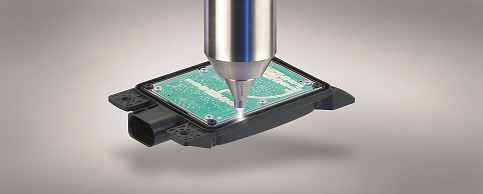
"Especially in electronics applications where the assembly is subject to high accelerations, components are sometimes fixed between solder pads with an additional adhesive dot. This is intended to help keep the component securely in its intended position," explains Coenen. Additionally, in the semiconductor industry Openair-Plasma has found its way. Typical vacuum plasma applications like treatment before wire bonding or die bonding being replaced by Openair-Plasma. The range of use and the speed of Openair-Plasma is offering much more economical and faster process opportunities for industrial applications.
Openair-Plasma has established itself as a reliable, cost-reducing standard process in the electronics industry. In order to treat components and entire assemblies with care, Plasmatreat has developed an Openair-Plasma nozzle especially for these applications which has been proven to work with a very low, harmless zero voltage input. This ensures gentle handling of electronic products.


Press Releases
- Parmi Expands Mid-Atlantic Sales Coverage with Cope Assembly Products
- Seika Machinery to Host SMI 2026 Webinar Series Session 2 on PCB Slicing Methods and Low-Stress Separation
- Pillarhouse USA Expands BarTron, Inc. Sales Territory into Indiana
- Mycronic appoints Peter Andries as General Manager of MRSI Systems and VP of Global Technologies Division