

The Basics of Thermal Profiling for Sensitive Components
Getting the right temperature is a balancing act, at times requiring fine juggling.
Creating a thermal profile isn’t as straightforward as it once was. PCBs are populated with a growing assortment of new packaging and technologies, introducing new challenges and their associated tradeoffs when it comes to creating the thermal profile. Usually, a conventional board consists of a mix of passive and active components in traditional packaging. Increasingly, boards are populated with µBGAs, µCSPs and µQFNs, as well as the larger BGAs, CSPs, and QFNs. Plus, there is continually smaller packaging like 01005s for passive devices.
Creating a profile for a board like this poses perplexing issues, since larger packages require more heat compared to smaller ones, and there are special considerations when it comes to package-on-package (PoP). Finding a temperature setting that’s acceptable to both larger and smaller packages, while juggling tradeoffs and special considerations, is a balancing act. It’s critical not to overheat smaller packages to avoid solder bridging. On the other hand, more heat needs to be applied to the larger BGA packages for solid solder joints and to keep from creating open solder joints.
After creating the thermal profile, the first-article board is run through reflow to determine whether the profile is good. At this point, x-ray inspection can be performed on both larger and µBGAs to determine whether issues exist: for instance, voids and other defects (Figure 1), such as whether BGA balls have collapsed per IPC standards. That first board informs and defines adjustments needed to the reflow profile.
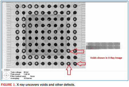
X-ray covers about 90% of the issues the process engineer views as a board goes through reflow. These x-ray visuals provide the roadmap for the type of adjustments that may be needed, such as a shorter or longer soak time or determining whether or not BGA balls aren’t collapsing. Then a higher peak temperature might also be needed for that particular board to reflow properly.
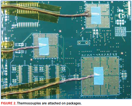
A variety of adjustments can be applied to the profile to accommodate large and small packages. In general, profiling involves making those adjustments on a board-by-board basis. The most common way to establish a profile is to first set a baseline and run it through the oven. To do that is a multi-step task. First, hermocouples are attached on these packages (Figure 2). To set the reflow oven temperature, a reading is taken to show the amount of heat these components
are exposed to when they go through the reflow oven at a certain speed. Once a reading is taken and the board exits the oven, the profile is refined by adjusting the pre-soak, soaking and reflow temperatures.
The right balance must be struck among soak time, peak temperature and reflow time. Soak time is fine-tuned to the critical components. A long soak time is normally not required for smaller packages. Larger packages, however, do need a longer soak time to provide sufficient time for paste flux volatiles to evaporate prior to reflow.
Part of that soak time review is to investigate differences in paste characteristics. These can drive the differences for each profile. Normally, for larger packages, the tendency is to target soldering issues by setting a longer and higher soak time. But at the same time, a lower peak temperature might be needed. This is done to avoid overheating smaller packages.
When profiling, ensure that peak temperatures are reached for the larger mass BGAs, but take care not to burn out the sensitive components. Simultaneously, temperature across the conveyor belt must be taken into account. That temperature can range anywhere from 2° to 5°C. Often, the edges of the PCB represent the coolest areas while in the oven. Therefore, they require even more heat if BGAs are placed on the edges of that particular board. For example, if a BGA on a particular board is normally set at the maximum peak temperature of 245°C, the tendency would be to bump it up. At the same time, however, keep watch on such components as electrolytic capacitors. For instance, by lowering their maximum peak temperature to around 235° or 240°C, that will prevent too much heat from being applied to those smaller components.
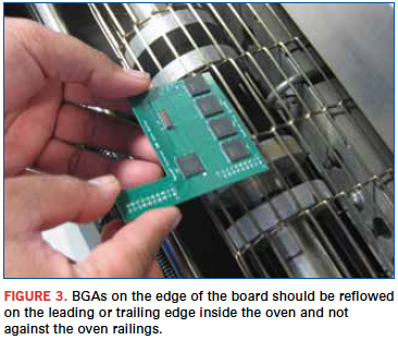
Also, railings on reflow ovens have to be taken into consideration. Temperatures closer to the railings tend to be several degrees cooler than the middle of the oven, thus having a huge impact on the profile. This can make the difference between a good and bad BGA reflow process.
There are several ways to resolve this. One is design and place BGAs away from the edge of the board. Ideally, BGAs will be located closer to the middle of the board. If this is not possible, an alternate approach is to make a reflow fixture for that particular board. The fixture would center the board in the oven to alleviate issues of cooler temperatures toward the edge of the board.
A major profile adjustment for process improvement is to turn that particular board 90° so that the BGAs on the edge of the board are either on the leading or trailing edge inside the oven, not against the railings of the oven (Figure 3).
Leveling the Heat
Take a PCB populated with BGAs, QFNs, CSPs and DFNs. Temperature readings are taken on these particular devices when a profile is being created. The reason is when higher temperature settings are applied on larger components, it’s important to ensure that the smaller components don’t overheat. Applying too much heat causes component failure or causes solder paste to exceed manufacturer’s required temperature readings. Efficiently and strategically spread the thermocouples across the board to achieve as accurate a reading as possible. This includes monitoring the middle and corners of the board.
Failure to achieve the right balance can lead to problems during testing or quality control. Some problems can be solder balls and delamination on the PCB. Solder balls usually occur when the board undergoes an excessive heating rate as it passes through the reflow oven. The reflow cycle is too long, and solder balls form throughout the board. Also, excessive heat can cause board delamination, compromising the reliability of the PCB.
Temperature setting is the trickiest part associated with balancing this trio of profile characteristics. Some components simply cannot handle higher temperatures or are highly heat-sensitive at certain temperatures. In the event a heat-sensitive component is used, the OEM should alert the assembler in advance and advise whether a SnPb or Pb-free profile is desired.
SnPb and Pb-free components are required on a board at times. Processing a Pb-free BGA based on a leaded thermal profile is certain to induce problems. A leaded solder’s melting point is about 25° to 30°C lower in temperature than that of a Pb-free material. In this particular instance, an open ball problem can result from using the wrong thermal profile.
The opposite is also true when processing a leaded board based on a lead-free profile, which requires considerably higher temperature. This mismatch can result in shorts or board warpage. BGA voiding is yet another defect that occurs. This is where the BGA is not 100% collapsed, and a void exists that results from one of multiple and different factors. A common adjustment to minimize voiding is a long, high soak and a lower peak temperature. The longer soak and high temperature is to provide sufficient time for the volatiles in the paste flux to evaporate prior to reflow.
Lack of BGA localized heating is another issue that might be encountered. This means that the BGA is not getting enough heat and the balls are not collapsing. Sometimes the thermal profile is not optimal, thus creating BGA voids. For example, a BGA that is typically heated to a maximum peak of 245°C might see the temperature increase slightly to ensure proper reflow.
PoP Profiles
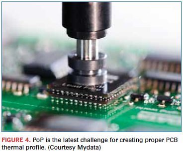
Package-on-package (PoP) poses a new challenge for creating the correct and proper thermal profile for a PCB (Figure 4). In this case, there are certain pros and cons to deal with. As of this writing, there are two popular ways, and either one can be a contract manufacturer’s preference since there is no standard profile for PoP. One involves separately reflowing one component on top of the primary one at the rework station or in the reflow oven. This process is performed before the PoP is installed on the board, and a separate profile is created for that component only. Once the top components are loaded onto the bottom ones using the rework station, all PoPs are installed on the PCB, and the entire board is run through the oven. The assembler needs to consider placement accuracy, paste or flux dipping and reflow warpage as critical areas for PoP applications.
The second method is soldering both components at the same time. In this instance, they are reflowed through the oven together and with the board. That particular profile could be used for every board with similar types of PoP components on that particular assembly. But most important is the level of research performed to achieve the correct profile and the steps taken to create it.
The two methods of PoP soldering have their respective pros and cons. The two methods are rework station and reflow oven. The advantage of using the rework station for PoP is that it targets the heat at one particular area. Nothing else is reflowed on that particular board. Consequently, temperature settings can be adjusted only for that particular area. As far as the engineer is concerned, this is a real plus, since no other parts on the board are affected as the PoP is reflowed onto the board by itself. This process works best mainly for small production runs like prototypes or small runs of five to 10 boards.
The disadvantage is the limited number of rework stations on the assembly floor. Usually, there’s one or two. So, the issue here is meeting delivery schedules since this process is not well suited for large-volume runs, unless multiple rework stations are on the manufacturing floor.
The advantage of using the reflow oven for PoP is the ability to make large-volume quantity runs on the production floor. The disadvantage is the fact that it
profiles the entire board, not just the PoP component. This means all the components on the board must be taken into consideration. And they also go through a thermal cycle.
In this scenario the process engineer encounters different problems in terms of different components handling different temperature levels. Therefore, a profile is necessary for PoP components and other sensitive components such as CSPs, QFNs, and DFNs. In effect, a general idea of a proper profile and defining the right temperature settings represent the key objective here. Here, it’s not so much as trying for a perfect profile, but one that’ll work for a particular board without creating any further issues with any type of package, like BGAs, LGAs, or PoPs.
Simon Ilustre is a process engineer at NexLogic Technologies (nexlogic.com); info@nexlogic.com.


