

2005 Articles
Mixed Technology Gets Selective
Selective and fountain soldering can reduce skips and opens over traditional wave processes.
Wave soldering is the predominant and oldest of technologies still commonly used for soldering PCBs. Wave soldering, which came about in the 1950s, is still the most efficient method for soldering through-hole components and is capable of producing high solder joint quality. With surface-mount technology came reflow soldering, developed as an alternative method of mass soldering components to PCBs. Reflow soldering also proved an efficient process capable of producing good quality solder joints. Most boards today are a combination of SMT and through-hole. These mixed-technology boards typically use both of the mass reflow processes in some form.
Typical mixed-technology soldering. The standard process for soldering mixed-technology boards is to reflow SMT components on the primary side and wave solder through-hole and secondary-side SMT components. Skips or opens have been an issue for wave soldering SMT ceramic chip components. Often, the wetting force of the solder is not sufficient to overcome gas entrapment which occurs at the junction of the component solder termination and the PCB land. To overcome this, a turbulent wave, also known as a chip wave, is used to ensure that these components solder properly. The mechanical force created by the turbulent wave is sufficient to displace any gases and force the solder into the junction of the component termination and land. When using a wave process for SMT components on the secondary side, an additional process is required to apply adhesive to hold the parts on the board as it goes across the wave. In addition to ceramic chip components, small outline transistors (SOT) and low-profile small outline integrated circuits (SOIC) components are sometimes wave-soldered; however, it is difficult to prevent defects on these components.
Paste and glue. To reduce the chance of opens on secondary-side SMT components and to eliminate the necessity of running a turbulent wave, a process of printing solder paste, applying adhesive, placing the components and then curing the adhesive while reflowing the solder paste can be used prior to wave soldering (Figure 1). This process offers the advantage of improved yields for the SMT components and reduces the amount of dross produced by wave soldering equipment with the elimination of the turbulent wave. When implementing this process, be sure to provide adequate space between solder paste deposits for the adhesive to prevent the adhesive from getting into the solder joint. Also, make sure the dispensing nozzle or nozzle stand off does not contact the paste, as this will result in a build-up of paste on the nozzle, causing the nozzle to clog. One way to ensure that solder paste does not clog the stencil, or that the paste does not get smeared by a subsequent stenciling operation, is to use noncontact adhesive dispensing equipment.
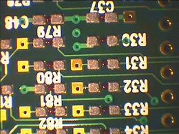 FIGURE 1: An assembly processed with paste and glue.
 |
Some stencil suppliers offer a stencil combination that permits paste and adhesive to be printed in separate operations. Printing adhesive on a board that has already been printed with paste is accomplished by using a stencil with a pocket that has been half-etched into the bottom side, around the area where the paste has been printed. This requires that the stencil for the adhesive be greater than twice the thickness of the paste stencil.
If adhesive is cured too quickly it will not achieve adequate strength. To avoid this problem, run a standard adhesive cure profile but do not reflow the solder paste. This will drive off volatile constituents in the solder paste, drying it and making it hard. The dried or hardened paste is then reflowed during primary reflow. Use an oven profile that will keep the board within the recommended temperature for the length of time recommended by the adhesive manufacturer to properly cure the adhesive prior to reaching reflow temperature.
lternative Soldering Processes
Reflow soldering typically provides the highest yields for SMT components while wave soldering provides the highest yields for through-hole components. Achieving high yields on leaded SMT devices using a wave solder process is difficult at best and almost impossible for fine-pitch devices. Other components such as tantalum capacitors are not rated for wave soldering. An increase in board complexity and density may necessitate the placement of these types of components on the secondary side and thus require the use of an alternative to standard wave solder processes. Alternative process options include selective wave soldering, selective solder, intrusive reflow and single point soldering.
Selective wave soldering. This process uses a wave pallet that shields all or a portion of the SMT components from the solder wave while exposing the through-hole components. This permits components that cannot go through wave soldering to be placed on the secondary side of the board and still wave solder the through-hole components. Selective wave pallets are typically made of a composite material that can repeatedly withstand the temperatures of wave soldering. The fixtures will have milled pockets that nest the SMT components, shielding them from the solder wave, and openings for through-hole components that expose them to the solder wave. The openings for the through-hole components need enough material surrounding them to provide a wall that can contact the board surface and act as a gasket to prevent solder leaks. This typically requires a clearance between through-hole and SMT components of about 3 mm. This area is called a keepout zone. The openings also require a beveled edge to permit solder to enter the pocket easily and permit a path for any air or gases to evacuate the opening as solder enters (Figure 2).
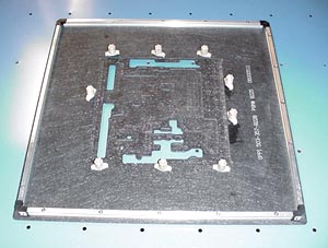 FIGURE 2: Selective wave soldering fixtures have openings with beveled edges to permit solder to enter the pocket.
 |
The main limitation of this process is component height. For a wave height of 6.35 mm, which is fairly typical, the material for the selective wave pallet will need to be 6 mm or less in thickness. The board is generally nested in the fixture so that the board surface and the fixture surface are at the same height. Approximately 2 mm of material needs to remain below the pocket that nests the components. Based on this, for a 1.5 mm thick board, the maximum component height would be 2.5 mm:
E.g., 1.5 mm (board thickness) + 2.5 mm (component height) + 2 mm (material below pocket) = 6 mm (thickness of pallet material).
Thicker material can be used for the wave pallet, permitting thicker components to be used, but this requires the wave nozzle to be lowered and wave height adjusted for proper clearance.
One advantage of selective wave soldering is that SMT components typically require more spacing when wave soldered than when reflowed. This is because components bridge much more easily, and a smaller component may be shadowed going through the wave by a larger component directly ahead of it. The improved density created by reducing the component spacing will usually more than offset the space lost due to the keepout zones required around the through-hole components. The quality and consistency of the solder joints of SMT components will be better when they are reflowed instead of wave soldered.
When using selective wave pallets, solder wave height will usually need to be lower than that of a standard wave solder process. The pallet is much thicker than a PCB, and the wave pressure will increase due to pallet thickness and the limited area of the openings for through-hole components. This process can use existing wave soldering equipment but will require investment in selective wave fixtures (Figure 3). The number of fixtures required will depend on production volume. For high-volume, low-mix, a continuous flow process is desirable. This will require enough fixtures to cycle through the process continuously. For low-volume, high-mix, it may be desirable to have fewer fixtures and run smaller batches. Return on investment is based on how many boards are projected to be built over the life of the product.
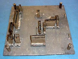 FIGURE 3: Selective solder nozzle plate fixture.
 |
Fountain selective soldering. Like selective wave, this process exposes only specific areas of the board to molten solder, such as the areas where through-hole components are located. Various types of selective soldering equipment are available. The predominant type uses a nozzle in the shape of the area to be soldered. Molten solder is pumped through the nozzle, contacting only components to be soldered. Multiple nozzles can be used to simultaneously solder more than one location. The board can either be lowered onto the nozzle as solder is flowing, or located over the nozzle as the solder pump is turned on, raising the solder level up to the board. The nozzle is designed to exhaust the solder so it does not contact adjacent components. The continuous flow of solder through the nozzle permits it to carry away dross or other impurities, much like a standard solder wave.
Another method is to use a solder reservoir formed in the shape of the area to be soldered. The solder reservoir is lowered below the surface of the molten solder of a solder pot and permitted fill with molten solder. Any dross or contaminants are skimmed off the pot surface prior to the reservoir being raised out of the solder. The PCB is then lowered onto the reservoir, contacting the leads of components being soldered and the PCB surface for the dwell time as programmed into the equipment. Raising one side of the PCB and tilting it as it is removed from the solder permits the surface tension of the solder to create a peel force that removes bridges, as with a wave soldering machine.
A third type of selective solder equipment uses a small solder fountain. The PCB is either lowered onto the fountain and then moved over it, or the fountain is raised to the board and moved across it to solder the intended locations. This process can be used when tall components are already attached to the side of the PCB to be soldered. The process might be required when connectors or other tall components are used on both sides of the board, making wave soldering impractical. Another advantage is a short cycle time when a high pin count is involved, as all leads can be soldered at the same time. This process requires an investment in equipment, fixtures and tooling. Selective soldering equipment ranges from less expensive tabletop units to inline equipment that includes preheat and fluxing capabilities (Figure 4).
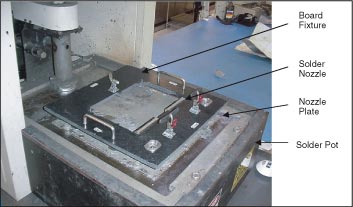 FIGURE 4: Selective wave soldering system.
 |
The board should remain flat during the process; therefore it is a good idea to use a fixture to hold the board throughout the process. To reduce thermal stress and activate the flux, the board needs to be preheated before soldering. This can be done by sitting the board just above the solder pot, or by using preheating equipment. Offline preheating equipment will shorten cycle time. Flux can be manually applied or automated fluxing equipment may be used. Spray fluxers are often used because the area where flux is applied is more easily controlled. The use of nitrogen can improve the quality of all three selective soldering processes.
Pin-in-paste. Pin-in-paste may be a desirable alternative to wave or selective soldering. It can be used in conjunction with an existing reflow process, eliminating the need for additional process steps. Pin-in-paste may be the least expensive alternative because of savings in equipment, fixtures and cycle time. However, it is recommended only under the following conditions:
Board thickness is 0.062" or less.
The through-hole component is reflow-compatible.
The lead pitch is sufficient to accommodate the solder volume needed.
The area around the holes (where paste is to be printed) is free of exposed metal, such as exposed vias.
Leads do not extend more than 0.040" beyond the board surface.
The body of the component is a minimum 0.010" above the pad so that the paste is not disturbed by the component when inserted into the board.
The hole-to-lead ratio is greater than 0.30 (use nominal dimensions)
H = hole diameter
D = lead diameter
L = width of lead in X
W = width of lead in YHole area = (H/2)2
Lead area
- For round leads = (D/2)2
- For square or rectangular leads = L*WHole-to-lead ratio = Lead area/Hole area (must be greater than 0.30)
The following should be kept in mind when designing the PCB:
Pad size should be minimized.
A hole-size for round leads of 0.012" larger than the lead diameter is recommended; for square or rectangular leads, a hole size of 0.010" larger than the maximum diagonal measurement is recommended.
Round leads rather than square leads are preferred.
When printing, the paste should be forced into the barrel, filling it completely. This may require additional squeegee pressure. Using a squeegee angle of 45° will also put more downward force on the solder paste, resulting in better hole-fill. Two passes with the squeegee may be necessary for complete hole-fill. Good PCB support is critical because of the greater squeegee pressure required.
After reflow the volume of solder is approximately 50% that of the solder paste deposited. This means that twice the volume of solder paste must be deposited as is needed to form the solder joint. IPC-A-610C requires a minimum vertical hole-fill of 75%. The following calculation can be used to determine if the solder paste volume being printed is adequate (where T=board thickness):
Print area = (print volume – hole volume)/stencil thickness
Print volume = (2) solder volume
Solder volume = hole volume – lead volume (for 100% hole fill)
Hole volume
- For round leads = (T)(D/2)2
- For square or rectangular leads = (L)(W)(T)
When implementing this process, review solder joint requirements with production inspectors. The solder joint fillet will typically be smaller than those produced by wave soldering, if there is a fillet at all. Board inspectors used to seeing solder joints produced by wave soldering may fail the boards simply because of a change in appearance.
Robotic soldering. Programmable soldering robots are capable of either linear or point-to-point soldering. Point-to-point solders one lead at a time, while linear moves down a row of leads in a single motion. Solder wire with a flux core is used to supply both the flux and solder. The heat source can be a soldering iron or diode laser. Dedicated fixtures are not required. A program for each assembly will need to be developed. This is a good solution for boards without a large number of leads or for low-volume applications. Cycle time may be a limitation of this process for high pin count assemblies, as it requires one second or more per lead.
Programmable selective soldering systems offer the advantage of being software-driven and not requiring dedicated fixturing. The equipment uses a precision nozzle that produces a small solder fountain to apply the solder. Either the nozzle is moved by means of an x-y-z servo-driven positioning system to the locations being soldered, or the board is moved over a stationary fountain exposing only the required locations to the solder. The equipment must be capable of applying flux to the areas to be soldered and preheating the board. Programming time will also be required for each new board to be run with this equipment and cycle time will typically be longer than a traditional wave solder process. The keepout zone between through-hole leads and SMT components will typically be about half that required by selective solder or selective wave processes.
Quality, cost and cycle time are important factors in selecting which soldering processes to use. Greater board complexity has driven development of many soldering alternatives. A particular production volume may make one soldering process more desirable. Some processes will require an investment in equipment or dedicated fixturing. Look at the costs of each alternative and perform an ROI analysis of the alternatives. An internal technology roadmap will help assess soldering challenges ahead, and may help accommodate any increase in board complexity that may result. Make sure the board design is compatible with the soldering process you wish to use. It may be better to determine a soldering strategy before board layout begins, to design-in process compatibility.
Bibliography
Bob Klenke, “Implementing Selective Soldering: A Cost-Effective Alternative to Traditional Mass Soldering,” SMTA International Conference Proceedings, September 2000.
Ralph W. Woodgate. The Handbook of Machine Soldering, 3rd ed., John Wiley, 1996.
Jonathan Wol and Adrian De’ath, “Emerging Trends in Selective Soldering Technology,” SMTA International Proceedings, September 2003.
Phil Zarrow, “Reflow Soldering of Through-Hole Components,” SMTA International Proceedings, September 1999.
Scott Buttars is a process engineer at Intel Corp. (intel.com); scott.k.buttars@intel.com.


Press Releases
- Changes in Incap’s Management Team: Incap updates its leadership model to support its growth strategy
- Niche Electronics Celebrates Completion of Florida Expansion
- Microscreen Names Nik Thomas Director, Expands Leadership Role Amid Continued Organizational Growth
- W&S Enters New Growth Phase Through Strategic Partnership and New Leadership