

2005 Articles
The Relationship of Components, Alloys and Fluxes, Part 2

In this installment, the author reviews the interactions of fluxes with components and alloys, respectively.
Ed.: This is the second of a two-part series. Click here to read Part 1, which looked at alloys and components.
Components vs. Fluxes
1. Solder Bumping
Solder fusion on wafer. For electroplated or evaporated solder bumps on wafer, the bumps need to be fused with spin-coated fluxes to eliminate the porosity of the bumps or round up the bumps. The fluxes required for this process often are not significantly affected by Pb-free. Fluxes used for fusing high lead solder bumps typically are also applicable for Pb-free, Sn-rich solder bumps, such as SnCu0.7 bumps.
Paste bumping on substrate or wafer. Solder paste bumping is a low-cost process for wafer bumping or pre-solder bumping on substrates. Fine powder is required, either type 4, 5, 6 or 7, depending on the pitch and bump dimension desired. Converting from SnPb37 to Pb-free (such as SAC) requires fluxes with better wetting and cleanability.
Ball mounting on wafer or BGA. Ball mounting on wafer or BGA employs printing or pin-transfer flux deposition, followed by ball placement and reflow. Converting to Pb-free solders results in a higher ball missing rate or misalignment rate due to the poorer wetting of Pb-free alloys. The flux residues are also harder to clean. Upgrading both aspects is essential for successful conversion.
Ball mounting on BGA socket. Solder bumping onto a socket is performed by printing paste or pin-transfer flux onto the pin head, followed by solder ball placement and reflow. The solder ball should form a bump by fully wetting the pin head, but wetting beyond the pin head can cause collapses. To confine solder wetting (and reduce cost), the surface finish of the pin is normally plated with nickel. For SnPb37 balls, it is not an issue to balance the wetting so that the ball wets sufficiently – but not excessively – on the pin head. For SAC solder balls, however, sufficient wetting often poses a challenge, and the flux activity needs to be improved.
2. Component Attachment
Small forms. Small form components such as 0402s or 0201s are prone to skewing, tombstoning or billboarding. Converting to Pb-free may lessen or aggravate the problem, depending on the alloy employed (Figure 4). To alleviate the problem and widen the process window, fluxes with slow wetting are desirable.
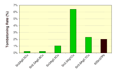 FIGURE 4: Tombstoning rate of solder pastes under vapor phase reflow. SAC and SnPb pastes were reflowed at 260° and 215°C, respectively.
 |
Large forms. Similar to the SnPb process, soldering large components or thick boards requires a long soak at reflow to minimize the temperature gradient across the board. However, if reflowing under air, soaking at around 200°C for Pb-free reflow will result in much more severe oxidation on parts and paste than soaking at the typical 160°C for SnPb reflow. This inevitably requires improved flux oxidation resistance and flux capacity.
Old components. In one special situation, the problem is associated with Pb-finished components but caused by Pb-free requirements. Due to expected shortages of Pb-finished components in the future, many of those parts are stocked for future repair or replacement needs. Those components can suffer excessive oxidation and hence poor solderability when stored beyond their recommended shelf life. In this case, an aggressive flux must be used to address this heavily oxidized surface finish.
No-flow underfill. No-flow underfill is a solution for enhancing the drop test performance of CSP solder joints, and has been adopted for portable devices. By dispensing no-flow underfill onto CSP pads, then placing the CSP and reflowing, the flux in no-flow underfill will clean the oxide, solder will wet the pad and form a joint, and the underfill cure will be completed at the end of reflow cycle.
No-flow has been employed successfully in production for Sn63Pb CSP processing. However, converting to Pb-free poses major challenges. First, Pb-free solder wetting is poorer, and non-wetting often occurs with no-flow fluxing chemistry, particularly in the case of OSP finishes. Second, outgassing of the Pb-free process also causes problems. One great challenge of no-flow underfilling is voiding and, accordingly, skew and chip drift caused by moisture. Sealing the space between the CSP and substrate with liquid underfill makes it very difficult for volatiles from the CSP and substrate to escape during reflow. This is particularly true for Pb-free CSP assembly, for which reflow temperatures are considerably higher. The third challenge is reworkability. Underfill cured at a higher temperature often is more difficult to rework due to a more thorough curing reaction.
Until recently, no-flow underfilling for Pb-free process has been a blank. This situation changed with the publication of Yin et al. on new materials that meet the crucial requirements. 14
Alloys vs. Fluxes
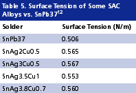
Higher activity fluxes. Pb-free alloys wet less well than SnPb37. This can be attributed to their surface tension being about 20% higher than that of eutectic SnPb (Table 5). Poor wetting results not only in poor solder spread but also in voiding, and hence becomes a major reliability concern. This inferior wetting power of Pb-free alloys will have to be compensated through the development of more aggressive fluxes.
Lower activation temperature of fluxes. Among Pb-free alternatives, BiSn52 and BiSn42Ag1 have a melting temperature around 138°C, and are particularly important for applications where parts cannot survive common soldering temperatures. To benefit from this low melting temperature, a flux with a low activation temperature is required. For a no-clean process, this presents a challenge, as higher activity at low temperature often demands the use of a more aggressive flux, while a benign flux residue after low temperature soldering process demands the use of a less aggressive flux.
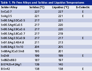
Compatibility with reactive elements. As shown in Table 1, some Pb-free alternatives contain reactive elements such as zinc or indium. This reactivity poses a compatibility issue between flux and solder in solder paste, and between flux residue and solder joints in a no-clean process. The compatibility challenge can be eased somewhat by adding bismuth into SnZn solder, and by keeping the indium content at or below 10%.
On the other hand, silver in solder has also been reported to catalyze dissociation of some covalent halide, which is often used as an activator in fluxes. This dissociated halide is reactive at ambient temperature, and thus can cause corrosion in solder paste. With silver being part of virtually all the vital Pb-free alloys, designing a proper flux chemistry becomes crucial.
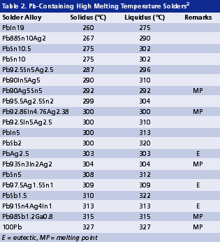
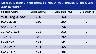
High melting temperature. The soldering process of high lead solders is often conducted between 300° and 380°C. Such temperatures are reaching the limit of thermal stability and cleanability of organic materials. As revealed in Tables 2 and 3, Pb-free alternatives for high lead solders virtually do not exist. On one hand, they are limited by the gap in alloy properties required compared with those of tentative candidates. On the other hand, even if some high melting alloys (Table 3) might be promising, it is extremely difficult to develop a flux that can survive a reflow temperature higher than 400°C. This limitation of organic materials in turn limits the possible options for high melt Pb-free solders.
Solder joint appearance and grain size. Compared with eutectic SnPb, the solder joint appearance of Pb-free alloys is typically dull and not smooth. This is attributed to the large dendrite formation caused by the strong crystallization tendency of high tin solders. Regardless, a joint with small grain size, or small dendrites, is still desirable for better creep resistance and fatigue resistance. Although the formation of grain is a metallurgical behavior of solder, the presence of flux on the surface of molten solder may affect the grain size by affecting the nucleation of solder. Hypothetically, fluxes that tend to induce the solder nucleation are expected to result in a greater number of grains, smaller dendrites and, consequently, smoother solder surface. The opposite would be expected for fluxes that tend to hinder the nucleation formation of solder. Yin et al reported that the microstructure of flip-chip SAC solder bumps can be affected by flux chemistry and cooling rate, with higher cooling rate resulting in a slightly finer microstructure in both grain and dendrite size. However, the effect of flux chemistry exhibits a greater effect than the cooling rate. Therefore, selecting a flux may not only affect solder wetting, but also may affect the microstructure of solder joints.15
Pb-free conversion is a complicated process. It impacts the electronics infrastructure, and causes interlinked chain reactions among components, alloys and fluxes. Although solder alloys may initiate that chain reaction, its impact on components and fluxes rebounds and affects the path of alloy developments. The interaction between components and fluxes further complicates their impact on alloys. Successful execution of Pb-free conversion requires the concurrent change and improvement of components, alloys and fluxes.
References
W. Yin and N-C. Lee, "Reworkable No-Flow Underfilling For Both Tin-Lead and Lead-Free Reflow Assembled Under Air,” SMTA International, September 2005.
W. Yin, N-C. Lee, F. Dimock, and K. Mattson, "Effect of Flux and Cooling Rate on Microstructure of Flip Chip SAC Bump,” SMTA International, September 2005.
Dr. Ning-Cheng Lee is vice president of technology at Indium Corp. of America (indium.com); nclee@indium.com.


Press Releases
- Adam Ryder appointed as Managing Director of Incap UK
- Metal Etch Services Opens New Motor City Facility to Meet Growing Midwest Demand
- Yamaha surface-mount line powers the future of specialized production at Inter-Company in Netherlands
- Matric Group Becomes the First U.S. Manufacturer to Deploy Panasonic NPM-GH Dual Lane SMT Technology