

2005 Articles
0.1 Cent RFID Chip Assembly?
Technologies to slash manufacturing costs for the ubiquitous tags are being aggressively pursued.
RFID applications are boundless. Technical analysis shows that broad-based applications of RFID will develop in two distinct phases. Phase 1, currently underway, is showing only marginal advances because RFID is superficially tacked onto existing business processes. The revolution will come during Phase 2: radical process reengineering and new RFID-centered business models. This phase will relaunch RFID as a new base technology. In addition, analysts say industry executives are focusing only on the price of RFID tags and when they will drop. Instead, industry should dedicate more creative resources to advancing manufacturing technologies.
Nevertheless, price is the significant benchmark for RFID tags to be accepted in broad markets. There is talk of the nickel tag, a fully functional passive RFID transponder for just a 5 cents per unit, which will be available by 2008. In 2003, the average price point of RFID tags was ten times this value. But now evidence of a new wave of technology enablers will drive down the production cost of RFID tags. This article looks at the cost of chip assembly and the various ways it can be implemented.
The method of assembling a chip onto a substrate (conventional die bonding technology) has been developed and optimized for decades. Based on this know-how, equipment vendors developed advanced die bonder for high-speed flip-chip assembly. Due to the huge demand predicted for RFID tags, a couple of visionary alternative approaches – for example, Fluidic Self Assembly1 and Vibratory Assembly2 – seem to offer a solution (Figure 1).
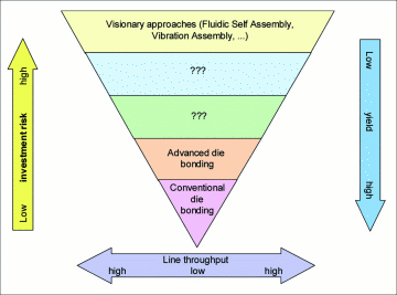 FIGURE 1: Benefits and tradeoffs of conventional and “visionary” approaches.
 |
The big advantages of conventional and advanced die bonders are their mature technology, low investment risk and high-yield operation. For the assembly of high-end flip-chip devices like DSPs and ASICs, an assembly yield of >99.95% is a standard target. For low-end flip-chip devices like RFID tags, a yield of 98% is standard, with 99% yield realistic provided all process and material parameters are well controlled, and 99.5% reachable in the mid-term timeframe.
This simple calculation helps explain the cost pareto of yield loss. A complete chip assembly line including adhesive application, flip-chip attach, curing, testing and slitting is currently available at a market price of <$1 million. With 7,400 hours of productive time, a line throughput of 10,000 UPH, and five years’ depreciation, the costs of chip assembly are 0.27 cents per tag. Assume a further 15 cents for the cost of an RFID tag and consider a yield loss of 2%. This calculates to a cost of yield loss of 0.3 cents, which exceeds the depreciation costs of the equipment. This example illustrates the high value of mature high-yield assembly equipment.
Direct and Indirect Chip Assembly
In the manufacturing of RFID tags, a basic distinction exists between direct chip assembly and indirect chip assembly (Figure 2). In direct assembly, the chip’s bumps are positioned and placed directly onto the antenna connections by means of flip-chip technology. The key advantage is a lower packaging cost, because this requires fewer process steps and consumes less material. However, despite the large antenna pitch, high throughput rates necessitate negligible indexing timing. Thus, with a conventional flip-chip bonder approach, the technology is not without its challenges. The bigger the bonding area of the antenna web, the more manageable those challenges are. However, the tradeoff with a bigger bonding area is a longer travel time for chip transport. A well-balanced dimensioning of the bonding area will result in a successful machine concept (Figure 3).
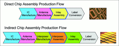 FIGURE 2: Direct and indirect chip assembly production flow.
 |
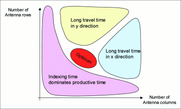 FIGURE 3: Optimal machine concept requires well-balanced dimensions of the bonding area.
 |
As an alternative, various manufacturers employ indirect RFID chip assembly. Indirect assembly, as a first process step, introduces a flip-chip interposer. In a subsequent step, at very high throughput and low cost of ownership, the interposer is mounted on the antenna, which can be done by crimping. Indirect assembly is advantageous especially for manufacturers that have no previous experience with bare-chip processing and do not want to invest in gathering the necessary know-how. At the same time, investment costs for the followup assembly step are significantly lower. The tradeoff here is higher packaging costs. Also, crimp connection quality is still a very controversial matter. Therefore, alternative methods such as soldering or adhesive interconnection methods are being used. Alternatively, the connection is facilitated after the interposer is glued onto cardboard and the antenna is applied in a second step via the printing of conductive ink over both cardboard and interposer.
Interconnection Methods
Users also must choose the type of interconnection method. Figure 4 shows various options available. In terms of RFID chip assembly, the most promising technologies are NCA (non-conductive adhesive) and ACA (anisotropic conductive adhesive).3 Because the pre-applied epoxy also functions as an underfill, the interconnection technology is very cost-effective, especially in paste form (NCP, ACP). The epoxy can be applied by screen printing or dispensing, whereby dispensing saves further costs because the process consumes less material. Bearing in mind that NCP is less expensive than ACP, the ideal interconnection technology seems to be dispensed NCP. Advantages of NCP are:
Easy, fast, low-cost processing.
High-quality interconnection.
No additional underfill.
Few process steps.
Low epoxy cost.
Heat compliant with low-cost substrate materials.
Usable for reel-to-reel applications.
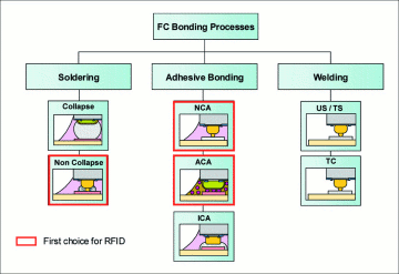 FIGURE 4: General flip-chip interconnection options.
 |
The feasibility of high-volume NCP production on flex substrate has been demonstrated in smartcard production, where the reliability requirements of flip-chip packages has been proven.
In addition, the non-collapse soldering process is used for RFID chip assembly. For example, gold bump soldering (GBS) benefits from the low bumping costs of the gold bump and the high quality of the intermetallic interconnection due to soldering.
To complete the picture: Collapse processes are not feasible because of higher bumping costs, thicker package profiles and the need for an extra underfill step, unless pre-applied underfill is used. The ICA process is inferior because it requires the extra underfill step. Ultrasonic and thermosonic require mechanically stable support from the substrate, which is not easy to achieve with low-cost materials like PET at thicknesses of 50 µm and below.
Chip Assembly Process Flow
As a final consideration, the various options of process flow for chip assembly must be understood (Figure 5). The classic flow, which has been used for NCP production, starts with epoxy application (screen printing or dispensing), followed by pick-flip-place (die attach). Curing takes place in a two-stage process: parallel lamination of a couple of dies in a heated press station (pre-curing)3 and final curing in an inline oven. Experience has shown that the number of process steps in the classic flow can be reduced by going with either the place and laminate flow, which does not need an inline oven for final cure, or the place and cure flow, which eliminates lamination in the heated press.
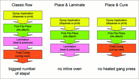 FIGURE 5: Types of chip assembly process flows.
 |
The place and laminate flow is widely used in RFID inlay production for NCP and ACP packages, but has its tradeoffs in line throughput. Figure 6 shows the achievable throughput of a heated press depending on the number of dies per index (to be laminated in parallel) and the curing dwell time, assuming 2 seconds for the non-productive time during index, open and close of the heated press.
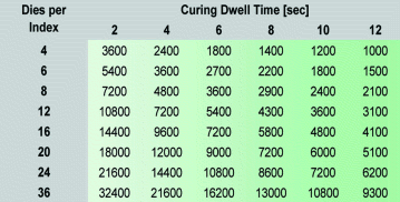 FIGURE 6: Throughput of a heated press for parallel lamination of die.
 |
Assuming a flip-chip bonder can process 7,500-10,000 UPH, depending on the antenna size, the line throughput can be essentially bottlenecked by the heated press, especially for production of big UHF inlays. This is a major reason why place and cure assembly solutions, standard for soldering processes, are the focus for planned investments.3-5
Returning to the question of whether a 5 cent tag will be realistic in the next few years, a widely used view of the RFID label’s cost budget is:
IC manufacturing costs (thinned, bumped, diced wafer): <2 cents
Antenna manufacture: <1 cent
Inlay assembly (including chip attach): <1 cent
Label conversion: <1 cent
Total: <5 cents
According to semiconductor manufacturers, RFID IC manufacturing for less than 2 cents will be realistic for high volumes.2,4,6 Also antenna manufacture and label conversion technologies are headed toward a cost target of <1 cent each. It is beyond the scope of this article to give a detailed picture of the cost map for all combinations of technological approaches for inlay assembly. Instead, the cost budget for a particular turnkey assembly solution is presented, which will clearly be a benchmark for all winning technologies in the future.
The benchmark is based on a UHF 4 x 1" inlay assembly process:
General assembly technology: High-speed flip-chip bonding
Chip assembly method: Direct chip assembly
Interconnection technology: Adhesive bonding/NCP
Process flow: Place and laminate
Epoxy application: Dispensing
Package test: Integrated
Slitting: Integrated
Line throughput: 10,000 UPH
The cost budget per tag for the inlay assembly process:
Depreciation costs for chip assembly: <0.22 cents
Depreciation costs for dispensing: <0.02 cents
Depreciation costs for test and slit: <0.03 cents
Operating costs: <0.06 cents
Adhesive costs: <0.05 cents
Yield loss: <0.30 cents
Total inlay assembly: <0.68 cents
Depreciation costs are based on five years and 7,400 productive hours per year; operating costs are based on $30/hr. including environmental costs, where each operator can serve five lines. Yield loss is based on 98% yield and 15 cents inlay costs.
Based on a two-year-outlook, the author proposes that equipment suppliers will be able to double the UPH of the assembly lines at constant equipment costs, and the yield should be increased to 99.5% while inlay costs drop below 5 cents. This results in the following mid-term cost budget benchmark for RFID inlay assembly:
Depreciation costs for chip assembly: <0.11 cents
Depreciation costs for dispensing: <0.01 cents
Depreciation costs for test and slit: <0.02 cents
Operating costs: <0.03 cents
Adhesive costs: <0.05 cents
Yield loss: <0.03 cents
Total inlay assembly: <0.25 cents
To manufacture RFID tags at very low cost, it is essential to understand the different technology approaches for RFID inlay production. The introduction of new visionary technologies will essentially depend on the yield costs which come along with these technologies. In this context, a benchmark based on mature turnkey production technology calculates inlay assembly costs of <0.68 cents at the current time, where chip assembly costs are below 0.22 cents. The two-year outlook is <0.25 cents for total inlay assembly and <0.11 cents for chip assembly.
References
John Stephen Smith, “RFID Inlay Assembly Technologies,” Smart Labels Conference Proceedings, June 2005.
G. Swamy, “RFID Tag Costing: Towards a 5¢ Tag,” TechSearch International Low-Cost RFID IC Packaging and Assembly Workshop, March 2005.
Achim Pajonk, “Variable Flipchip-Montage for High Volume,” Productronic, April 2004.
N.J.A. van Veen, “RFID Technology Development Activities at Philips,” TechSearch International Low-Cost RFID IC Packaging and Assembly Workshop, March 2005.
J.U. Fuhrmann and W. Reinert, “FliBuSi: Flip-Chip-Bonding for Ultra-Thin Silicon – Verfahren zur Verarbeitung dünner Siliziumchips,” Productronic, November 2003.
G. Swamy and S. Sarma, “Manufacturing Cost Simulations for Low Cost RFID Systems,” Auto-ID Center, February 2003.
Bibliography
P. Stampka, “FCOS: Flip Chip Technology for Smart Card (Contact Based) Modules,” IEEE CPMT, February 2005.
Hugo Pristauz is manager, advanced technology and business development, RFID, Datacon Technology GmbH (datacon.at); hugo.pristauz@datacon.at.


Press Releases
- Changes in Incap’s Management Team: Incap updates its leadership model to support its growth strategy
- Niche Electronics Celebrates Completion of Florida Expansion
- Microscreen Names Nik Thomas Director, Expands Leadership Role Amid Continued Organizational Growth
- W&S Enters New Growth Phase Through Strategic Partnership and New Leadership