

Designing for PCB Manufacturability
 Making a board producible is entirely in your hands.
The goal of a good documentation package is that it is complete and coherent enough to proceed with the job without any explanations, waivers, errata or feedback of any kind. It doesn't always work that way, particularly when more than one vendor is involved. The fab drawing is more of a baseline from which they will all deviate to one degree or another. Even using the same vendor all the time is no guarantee that the DfM data come back immaculate.
The foundational aspect of PCB fabrication is a plausible phototool. That final imagery is derived from the artwork that you sent their way. What we know as global micro editing is where the phototool is crafted from the ECAD data. The artwork is more like a starting point.
Etch compensation – pre-distorting the artwork.The first item on the CAM operator's list is dealing with etch compensation. The traces and other geometry that appear on the board are what's left behind after the etch process. First, they must drill and plate the holes with copper. That's done prior to etching and adds a measure of copper to the entire panel. Only then do they mask off the circuit pattern that is not to be removed.
This means that the amount of copper to be etched away is a total of the beginning copper and whatever is added during via plating. You'll see that outer layers tend to have more copper than innerlayers. The exact amount of copper required in the barrel is often a technical question from the fabricator. Literally everything else flows from that number.
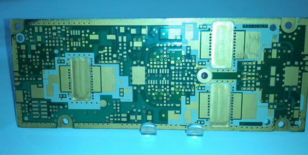
Figure 1. A showcase board that Sanmina had in its booth for years after it was produced. It's a heavy copper board with controlled depth slots and special patented vias along the slot edges. Five meetings came before tape-out on this radio board. (Image credit: Author)
Once the via plating deviation is approved, the fabricator can figure out how much to alter the photoresist so that the result comes out similar to what the artwork provided in the first place. The tendency is to make the tooling wider than the original to account for the profile of the trace as the chemistry forms the air gap. On balance, a narrow line is easier to etch than an equally narrow air gap.
Stackup tolerances: It's not a perfect world. The actual routing area on a board is slightly less than the board outline. The no-man's land permits random variation in the process. Every aspect of the board is ruled by some kind of tolerance. It's up to the designer to decide whether to believe the component data sheet of the fabricator's technology roadmap. You're likely the only one aware of some of these routine decisions.
The designer also must be a filter for requests that are out of touch with the fabrication limitations. It's true that the capture pads can be suppressed on layers where they do not connect. For Class 1 and 2 boards, the drill can cut a hole extending beyond the diameter of the "unused" pad. As much as 25% of the hole's diameter can wander outside the edge of the pad on any given layer and still meet IPC Class 2 specifications. Deleting those unconnected pads does not mean that the clearance (anti-pad) can be reduced.
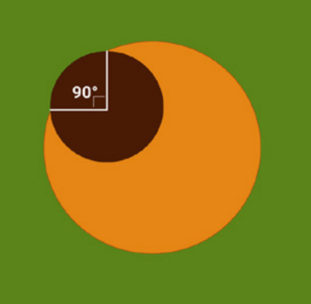
Figure 2. The brown circle indicates the maximum overlap of the hole and the edge of the capture pad for Class 2 boards. (Image credit: Sierra Circuits)
The case of sequentially stacking microvias to solve high-density interconnect (HDI) layouts is different in that all layers will usually plate up. Button plating is more likely to be found when creating flex circuits. The laser vias are ablated then plated one layer at a time in any case. The smaller via geometry only emphasizes the positional differences from layer to layer. Good thing lasers retain their edge and precision all day long.
The important metric becomes the aspect ratio of the via. The fabricator can make a deep and narrow hole with a laser, but can't plate it unless it's shallow. By shallow, take it to mean a hole that is wider than it is deep. Thin dielectrics are required to achieve the full potential of HDI technology. A byproduct of that is the calculated line width for controlled impedance gets narrower as the thinnest dielectric materials are implemented.
A larger annular ring is the No. 1 thing you can give your fabricator. One of the key differences between Class 2 and Class 3 boards is the allowance of the break-out of the drill on Class 2, while Class 3 maintains a complete annular ring. The whole process of piling one layer above the next gets easier as pad size increases relative to hole size. The drill pattern repeats with the same precision provided the bit is sharp.
The artwork also aligns over the entire stack with random misregistration. The repeatability of the tooling holes vs. the tooling pins governs the stackup uniformity. Every panel is unique in its imperfections. No matter the class, larger capture pads lead to more robust printed circuit boards.
It's harder to prevent things you can't see. Just like screen printing t-shirts, one color is easy whereas multiple colors (layers) increase the chances of misalignment. Thus, the solder mask openings benefit from expansion over the size of the copper pad, typically 50µm all around. The edge of the mask opening should then see another 75µm before any silkscreen is applied. Using a line width of zero for the silkscreen will make it harder to judge if the edge of the line avoids the edge of the mask opening.
Think of the layout as a digital twin of the fabricated board. Think of how small bits of a screen-printed t-shirt flake off in the wash. Avoid using a period or other tiny bits of punctuation. As silkscreen features get smaller, a circle becomes better than a cross as both become a little blob of ink at a certain point. Solder mask also has a minimum feature size before it becomes a sliver that will not adhere to the board.
Part of the DfM ethos is to keep prices down. In the bigger picture, cutting costs on a bare board only to have it fail in assembly, test or in the user's hands is sequentially worse. Size matters to most marketing teams; find the balance. Some boards may require laser printing, others may get away with no silkscreen at all.
The bare board is the foundation of the end-product. The product is only as good as the underlying printed circuit board. Making it producible is entirely in your hands. The penalty for failure can be severe in terms of the company's results. When someone asks for a feature that is not manufacturable, then it's up to you to speak for the fabricator. You're the advocate for the board and that fits with the fact that it's your name at the top of the list in the title block. Own it.
is a career PCB designer experienced in military, telecom, consumer hardware and, lately, the automotive industry. Originally, he was an RF specialist but is compelled to flip the bit now and then to fill the need for high-speed digital design. He enjoys playing bass and racing bikes when he's not writing about or performing PCB layout. His column is produced by Cadence Design Systems and runs monthly.


Press Releases
- Adam Ryder appointed as Managing Director of Incap UK
- Metal Etch Services Opens New Motor City Facility to Meet Growing Midwest Demand
- Yamaha surface-mount line powers the future of specialized production at Inter-Company in Netherlands
- Matric Group Becomes the First U.S. Manufacturer to Deploy Panasonic NPM-GH Dual Lane SMT Technology