

Printing Analog Circuit Elements Directly on the PCB
 Prepare yourself for unusual circuit patterns.
There is no free lunch when it comes to populating a printed circuit board. Every part has a cost and a failure rate. One of the first projects of my career was a pulse-Doppler surveillance radar called PSTAR. In typical military jargon, that acronym stands for “Portable Search and Target Acquisition Radar.”
My part was the amplifier module that was subdivided into various blocks for easy field service. One of the sub-blocks was a 20dB coupler. It lived inside its own hermetically sealed aluminum housing. The PCB inside had two traces that ran alongside each other, giving the circuit four ports with feedthroughs to the outside world. SMA connectors and semi-rigid cables wired the various modules together.
My responsibilities included the little housing for the coupler, the overall mechanical packaging and all the semi-rigid cable drawings, as well as the RF amplifier. The control board was the only part designed by an external vendor. Meanwhile, the PCB for the coupler had no more than a single 50Ω termination resistor and the feedthrough connectors. We did not yet have PCB design software at that company, so this was done with AutoCAD.
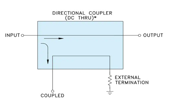
Figure 1. The typical broadside coupler will have the ports organized as shown while a quadrature hybrid coupler will flip the output and termination port, which requires two layers on the PCB. (Source: Mini-Circuits)
That was back in 1990, but I still remember that simple board that was little more than a mirrored shape. At its core, the coupler is represented by the two transmission lines running parallel for a distance equal to a quarter of one wavelength of the resonant frequency, which was 13cm; somewhere in the 900MHz range. That type is known as a directional coupler.
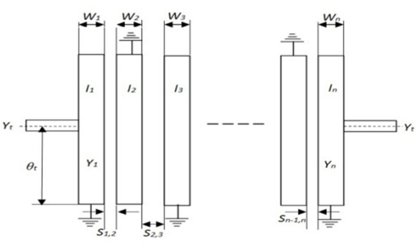
Figure 2. The interdigital bandpass filter bears a strong resemblance to this diagram. (Source: International Journal of Scientific & Engineering Research)
Quadrature hybrid couplers. Another type, a quadrature hybrid coupler, can also be printed, although the transmission lines are created on adjacent layers. The trick here is that layer-to-layer registration becomes important, particularly as the lines get thinner. Due to stackup realities, the 50Ω stripline may be something like 100µm. Now, if the layer-to-layer misregistration is 25µm off in the direction that affects the two lines going belly-to-belly, then the coupling will drop off 25%.
Facing this exact problem, I went to the PCB West conference carrying a rolled-up blueprint with fab notes regarding the layer-to-layer constraint among other challenges. This was rather unexpected among the PCB fabrication vendors on the exhibition floor, but they would all stop what they were doing when I unrolled that D-size print. Most of the vendors had to pass on the chance to do this job but a few would take on the precise registration spec by imaging both sides of the core simultaneously.
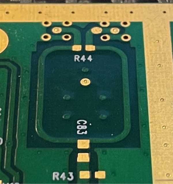
Figure 3. A Wilkinson divider circuit as part of a feed-forward correction board that controls the amplifier at the base of a cellular tower. In many cases, the solder mask is opened, leaving only a thin dam to contain solder on the SMD pads. (Source: Author)
Interdigital filters. Another type of component that can be etched rather than placed on the board is the interdigital filter. This circuit element owes something to the broadside coupler element. Microwave signals propagate across fairly wide gaps, making this a more manufacturable item, which would be printed on the outer layers. The stub length is again determined by the 1/4 wavelength. The rest is a complex mathematical formula.
Wilkinson combiners/dividers. When you want to combine or divide RF transmission lines without inducing a phase shift, the Wilkinson element comes in handy. To be fair, this does require a balance resistor at the business end. As you may have guessed, the length of the lines is determined by the resonant frequency (wavelength) of the radio. We’re looking at about 3cm on each branch in this case.
Finally, a printed inductor. This one was a bit tricky since the trace goes from a signal net directly to ground. The squared off spiral inductor in Figure 4 extends from the transmission line and ends with a via to ground. Of course, it is also surrounded by ground pour that we don’t want shorting to the signal path. A route keep-out around the edges provides that assurance.
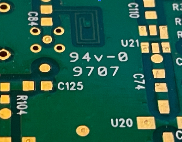
Figure 4. The same PCB as in Figure 3, and noted for being the first layout I did using Cadence Allegro. The 1997 date code puts this in the early 3G CDMA era. (Source: Author)
It seems that analog boards lend themselves to unusual circuit patterns. Matching networks can include tuning stubs that can be cut or extended with little copper tabs. Stray noise can be isolated with a band of grounded copper. Thermal dissipation can be enhanced with a tightly spaced grid of vias on an exposed copper plane. Replacing resistors, filters and heatsinks may take some PCB real estate, but earns it back by reducing the BoM cost, along with the potential for mitigating assembly defects.
is a career PCB designer experienced in military, telecom, consumer hardware and, lately, the automotive industry. Originally, he was an RF specialist but is compelled to flip the bit now and then to fill the need for high-speed digital design. He enjoys playing bass and racing bikes when he’s not writing about or performing PCB layout. His column is produced by Cadence Design Systems and runs monthly.


Press Releases
- Adam Ryder appointed as Managing Director of Incap UK
- Metal Etch Services Opens New Motor City Facility to Meet Growing Midwest Demand
- Yamaha surface-mount line powers the future of specialized production at Inter-Company in Netherlands
- Matric Group Becomes the First U.S. Manufacturer to Deploy Panasonic NPM-GH Dual Lane SMT Technology