

National Semi Consortium Starts with Next-Gen Workforce Focus
 Government-funded organization hopes to knock down barriers to commercialization.
The American Vacuum Society (AVS) held its annual conference in Portland, OR, with roughly 2,000 in attendance for the November meeting. The conference included many technical presentations by students, faculty and industry on cutting-edge issues associated with materials, processing and interfaces.
Among the highlights this year was a special session on the Chips Act. The session on the Chips and Science Act Implementation for Microelectronics (including workforce) was moderated by Dr. Alain Diebold, SUNY Polytechnic Institute, and Dr. Tina Kaarsberg, US Dept. of Energy Advanced Manufacturing Office.
The first invited talk was given by Dr. Jay Lewis, director, National Semiconductor Technology Center (NSTC). NSTC is a public/private consortium authorized and funded by the US government to serve as the focal point for research and engineering throughout the semiconductor ecosystem, advancing and enabling disruptive innovation to provide US leadership in the industries of the future. Dr. Lewis announced the incorporation of a new nonprofit entity, SemiUS, to operate the NSTC. SemiUS will work in partnership with the US Department of Commerce to develop and implement a wide variety of programs to fulfill the mission of the NSTC consortium. The focus is on building a strong semiconductor research and development ecosystem in the United States.
Under the Chips for America program, $39 billion in incentives has been allocated to invest in US production of strategically important semiconductor chips, and ensure a sufficient sustainable and secure supply of older and current generation chips for national security purposes and critical manufacturing industries. To strengthen US semiconductor R&D leadership to catalyze and capture the next set of critical technologies, applications and industries, $11 billion is allocated. Funding of $2 billion for DoD Microelectronics Commons is targeted to establish a national network that will create direct pathways to commercialization for US microelectronics researchers and designers from “lab to fab.” Workforce development initiatives underpin all programs. There is a focus on reducing barriers for the introduction of disruptive technology in the semiconductor industry. Gaps to be addressed include obstacles for startups and disruptive technologies (including chip design, process technology, metrology or materials), access to advanced foundries (often for R&D), and workforce. Figure 1 illustrates big picture investment categories.
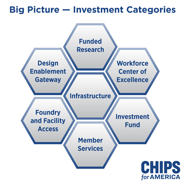
Figure 1. US Chips Act investment areas. (Source: NIST, US Department of Commerce)
David Anderson, president of the New York Center for Research, Economic Advancement, Technology, Engineering, and Science (NY CREATES), detailed the latest activities in research and workforce development. Global research cooperation includes relationships with Interuniversity Microelectronics Centre (IMEC) in Belgium, the Korean Institute for Advancement of Technology (KIAT), Israel Innovation Authority and Silicon Saxony and Fraunhofer (both Germany). Research areas include neuromorphic computing, integrated photonics, test, assembly and packaging (TAP), quantum technologies, magnetic random access memory (MRAM) technology, advanced process technologies and integration, power electronics, and heterogeneous integration. Industry research partners include large companies such as GlobalFoundries, TEL, Wolfspeed and NXP, as well as startups and small and medium enterprises. Workforce developments include programs with universities, high schools and training programs for veterans.
Intel’s Dr. Steve Pawlowski’s view on the 1000x Performance Efficiency Goal highlighted architecture changes for future computing, and focused on the importance of, and relationship between, software and hardware.
Dr. Vijay Raghunathan of Purdue University described programs related to workforce development at the university, which successfully increased the number of students entering engineering by creating a course for freshman that introduces them to the industry. Student-run career fairs and industrial roundtable job fairs are among the methods used. The school’s goal is a 500% increase in the number of engineering students in five years. Purdue’s high school summer camps that introduce technology to potential students is one way to increase the number of students in the pipeline.
Power efficiency. I opened my presentation, “Saving Power with New Designs and and Chiplets in the New Era of Advanced Packaging,” with a quote from Dr. Lisa Su, CEO of AMD, who asserts “energy efficiency is the most important challenge of the next decade.” A chiplet is not a package, I noted, but rather a new IC design approach with multiple package options including laminate substrate (with and without the use of silicon bridges), silicon interposers and redistribution layer (RDL) structures (with and without bridges). One of the most dramatic examples of improved power efficiency is 3-D stacking of chiplets using hybrid bonding. TSMC has published data indicating that its hybrid bonding process with 9μm pad pitch provides greater power efficiency than side-by-side configurations interposers or 3-D stacking with microbumps. AMD uses TSMC’s technology for its 3-D V-Cache memory on logic stacking and reports a 3X interconnect energy efficiency versus 3-D with microbumps. This technology has been deployed in volume production for AMD’s server and desktop processors for several product generations, as well as gaming and graphics applications. AMD’s new AI product, MI 300, will use logic-on-logic stacking for GPU and CPU chiplets using TSMC’s process. It will provide an even greater performance-per-watt improvement.
Many companies, including Intel and IBM, are working to develop 3-D hybrid bonding options. Challenges include the elimination of particles that can cause voids, careful consideration of thermal design and process developments. Co-packaged optics (CPO) is also under development and has the potential to provide 30% or more power savings in the datacenter. Examples of chiplets designs in silicon photonics applications have been demonstrated by Ayar Labs and Intel, Broadcom, Cisco, Marvell and others. TSMC is supporting CPO developments with its Compact Universal Photonic Engine (COUPE) that uses 3-D stacking with TSV in the photonic IC. The ecosystem is being developed and technology advancements are underway to enable deployment of CPO.
is president of TechSearch International (techsearchinc.com); jan@techsearchinc.com.


Press Releases
- Forwessun Expands Testing Capabilities through Strategic TRI Alliance
- Federal Electronics Expands Advanced Manufacturing Capabilities to Support Military and Aerospace Cable Assembly and Wire Harness Programs
- Altus Continues Irish Growth with Expansion of Engineering Team
- Kevin Castonguay Joins MicroCare as Senior Director of Marketing