

Cold Underfill Component Removal
Newly developed, dedicated purpose precision milling machinery simplifies rework.
BGAs, CSPs, flip chips and other component packages on handheld devices are commonplace today in consumer, military, and industrial products such as tablets, smartwatches, and handheld computers. These handheld products, along with transmission control modules, cameras and image sensors in the automotive sector, use underfill to withstand mechanical shock or impact that takes place when devices are dropped or struck. Underfilling these component packages creates a compliant layer between the package and printed circuit board that increases the reliability of the interconnections even when subjected to outside forces.
Underfill is a polymeric material used to fill the gap between the PCB and underside of the electronic component package, thereby surrounding and protecting the solder joints. This material boosts the reliability of the component, which is subject to mechanical impacts and shocks by distributing the forces. Thermal stresses caused by the coefficient of thermal expansion (CTE) mismatch between the component and PCB are lessened using underfill. Typically, underfills have a high modulus (E) matched CTE with respect to the solder, as well as a high glass transition temperature (Tg). Underfill dampens and distributes the stress more uniformly on the solder joints, thereby increasing interconnection reliability. As pitch of components such as CSPs becomes tighter, the standoff height between the bottom of the device and PCB lessens, thereby reducing the PCB level reliability.1
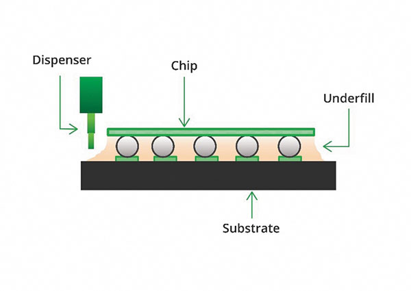
Figure 1. Underfill is dispensed under advanced packages such as BGAs and CSPs to increase reliability.
Challenges with reworking of underfilled components on PCBs include but are not limited to the following:
- Many underfills, when softened at elevated temperature, displace solder joints and components, resulting in defects.
- The economics of underfill removal are not worthwhile. Low yields and the prohibitive cost of long processing times for experienced “high touch” rework are the norm.
- Potential physical damage to the PCB is a risk as the underfill rework process may cause laminate damage, mask destruction and lifted pads, reducing assembly reliability (FIGURE 2).
Non-reworkable underfills, which exhibit excellent stability at temperatures much higher than the liquidus temperature of lead-free solders, are difficult to rework using standard PCB rework processes and tools. This eliminates the possibility of using a thermal- or thermal/mechanical-based rework process.
OEMs object to use of chemical “softening agents,” which can aggressively attack the PCB and may damage components, boards and other materials.
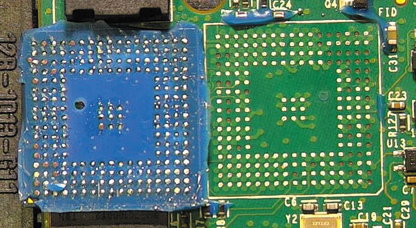
Figure 2. Underfilled BGA pulls up pads upon removal of component in a non-reworkable underfill.
These challenges were confirmed in the iNEMI 2019 Roadmap2, in which the Rework section outlined that one of the most significant rework challenges is reworking where there is minimal or zero clearance between adjacent parts near an underfilled area array device.
Current Underfill Rework Process Methods
Hot air or IR heat source. The first step in preparing a board for rework is to bake it per J-STD-033 to prevent moisture-induced failures. Underfill provides a strong adhesive force on the underside of the component that needs to be “broken” to lift the component on the rework station. This means the board needs to be properly fixtured and secured. Bars, pillars or custom pallets are used to hold boards in place during the removal cycle.
Like all rework processes, a proper temperature profile is needed, with thermocouples embedded at key locations such as the corners of the device, the die, and the corner and middle solder balls. The proper removal profile should minimize the force necessary to break the bond between the underfill and board. If temperatures are too low, excessive force will be required, and BGA pads will have a propensity to lift during the removal process. A profile that is too hot or long may cause other issues, such as component or board warpage, and underfill pushing solder joints off the pad.
Several methods exist for breaking the force between the underfill and board or the underfill and component. In some cases, the rework technician manually cuts through the underfill with a (heated) knife. Once completed, the tech will pry the BGA loose from the board. Various rework nozzle designs can aid in the removal. In some cases, the nozzle can be twisted during the removal process. Alternatively, a special gripper nozzle can simultaneously grab and lift the component. Once the component is removed, underfill residue is left behind. Tacky flux is applied with the heat from a soldering iron or hot air tool to soften the remaining residue. This mixture is best removed with solder braid. This process is not only time-consuming, but may lead to damaged mask or lifted pads. In addition, the potential damage to neighboring components can result.
After being dressed, the site is cleaned using IPA and a wipe. The site is now ready for placement and reflow of the replacement component.
Chemicals. Commercially available organic solvents can dissolve and remove a cured underfill from underneath an area array package. In this rework scenario, the board is placed into the softening agent, which may or may not have to be at an elevated temperature. The overriding concern with this technique is the unknown impact of the chemical on components and the PCB. After exposure to the softening agent, the component is subjected to hot air or IR rework sources to remove the component.
Laser ablation. Another technique for removing the component utilizes selective laser ablation of the component, underfill material and solder. This process involves careful laser processing and source selection, as the wavelength of the laser must be tuned to multiple material absorption spectra to ablate the material. In addition, the depth of the laser needs to be carefully controlled to avoid damage to neighboring components or the PCB.
Refined Cold Milling Process
One of the other techniques to remove underfilled components is through a “cold” process. The component is milled from the PCB, leaving a solder remnant of a few thousandths of an inch. The remnant solder becomes the pre-tinned pads for the replacement component.
Alternatively, the milled location can be site-prepped using a soldering iron and braid to remove remnant solder. This process ensures components near the rework location do not experience solder reflow temperatures. This eliminates solder from being “squirted” out by the softened underfill, which can cause solder shorts or opens.
Previous milling methods have used retrofitted commercially available mills with some modifications to accomplish this mechanical “cold” removal. While the milling machines could be grounded, static charges generated during the milling operation could cause ESD damage. Solder, component and other debris could cause potential reliability risks if permitted to spread to other areas of the PCB. Couple this with the vibration of the milling operation and the subsequent risk to cracking of solder joints made this technique a last-ditch approach for underfilled component removal. The machine operator and rework technician masking the board of any potential foreign object damage (FOD) and site preparation must be highly skilled to work on such projects.
Newly developed, dedicated-purpose precision milling machinery simplifies the process of component removal via a “cold” removal milling process. The commercially available machinery today consists of the following:
- Rework software, including structured machined programming, eliminates the need for a highly skilled CNC programmer/operator to run the machines. The x and y dimensions generate the milling pattern. Fiducials on the PCB read by the machine sensors and all precision alignment are locked onto these coordinates. Irregularly shaped features like those of an RF shield are easily programmed into the machine.
- A vacuum chuck that does not permit metal shavings to be dispersed from the rework area eradicates shielding of each rework location.
- An integrated active ionization source, which reduces the potential incidence of charging due to the milling operation.
- Vacuum-based board holding and support are used to ensure coplanarity of the milling surface relative to the PCB.
- Laser-based automatic multipoint measuring scheme to determine the true accuracy of the component, board and tooling offsets. In some cases, this permits cuts to within 0.001" from the board surface.
Case Studies
Under-the-hood automobile module. In an application requiring removal of a BGA (FIGURE 3) directly on the other side of an underfilled component, heat-based component removal techniques did not work. As soon as either hot air or IR energy was directed onto the component to be reworked, the temperature on the other side of the PCB rose to a point where the underfill material softened. Once this occurred, the underfill expanded, pushing neighboring reflowed solder around the PCB. This action led to solder balls formation, disturbing components (FIGURE 4).
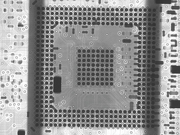
Figure 3. Initial x-ray of BGA rework location of under-the-hood module..
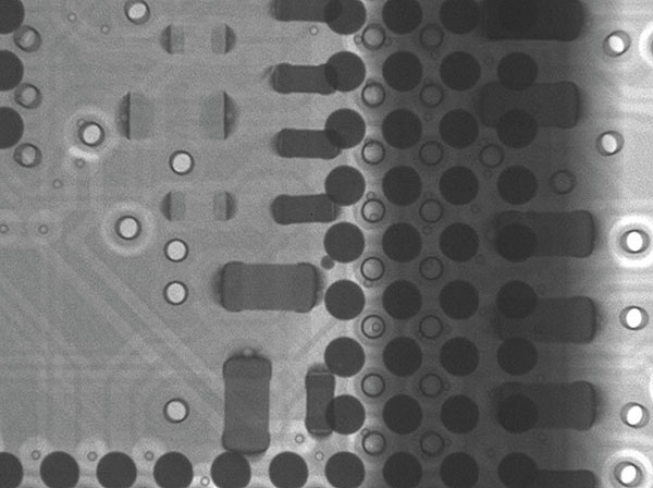
Figure 4. Neighboring passive components shifted and solder balls formed during reflow of underfilled components.
Using the cold removal process on the BGA, the neighboring underfilled components do not experience the underfill shift or push around components or solder, resulting in a much higher yield (over 90%). At the same time, this obviated the need for highly skilled and experienced BGA rework and repair technicians to fix the problem. The component was milled off using a 30-mil diameter mill at 15,000rpm spindle speed and a horizontal travel of 2mm/sec. The milling routine was optimized using a variety of cut depths. This included taking larger depths of cut initially as the cutter moved through the component body, and then smaller depths of cut with a 20-mil diameter bit using a slower cut speed. After several cuts, the distance from the final milled surface to the PCB surface was, on average, 2.2 mils (FIGURE 5). Once the BGA location was milled, the component was placed using a paste flux stencil printed on the replacement BGA. It was reflowed using a split vision hot air rework station with a 60 sec. time above liquidus (TAL) profile. X-ray imaging along with dye-and-pry analysis confirmed the previously disturbed components were free of soldering anomalies.
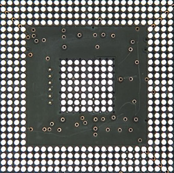
Figure 5. BGA of under-the-hood PCB milled to 2.2-mil height.
Communication system for retail. A handheld retail communications PCB (FIGURE 6) had underfill applied at a variety of component locations. The BGA rework location was also underfilled. The adhesive properties of the non-reworkable underfill caused the underlying BGA pads to lift off the board during hot air removal (FIGURES 7 and 8). Removing the remnant solder and underfill from the BGA location resulted in numerous lifted pads. While some pads were “no connects,” others that were lifted most often were connected to either vias or lands, making the repair time-consuming and therefore “beyond economic repair.”
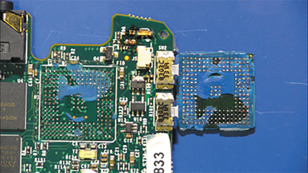
Figure 6. Underfilled BGA rework location for retail communication system.
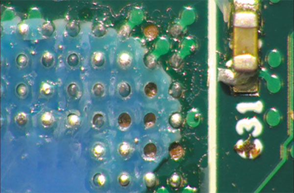
Figure 7. Lifted pads after removal of underfilled BGA.
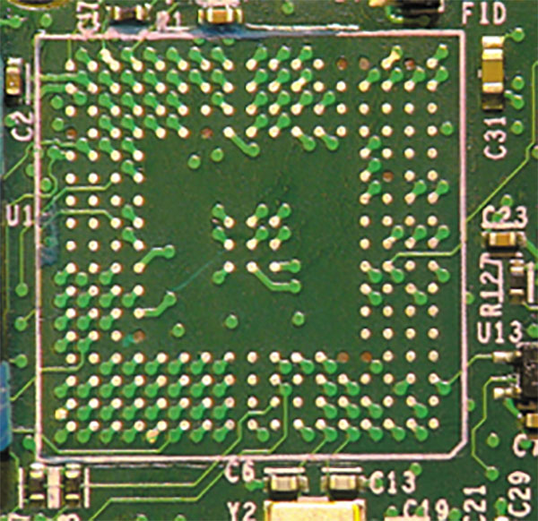
Figure 8. Lifted pads after removal of underfilled BGA.
After consultation with the OEM, more samples and further process development yielded a cold removal process using a commercially available precision milling system. After two gross depth cuts and two refined milling profiles, the component was removed with 2.5 mils of solder remaining on the pads. The milling process resulted in no pads being lifted. In addition, this semiautomated process took some of the “art” out of the rework process, thereby improving yield and throughput. The component removal time of 14 min. added 7% to the cost of the rework service. The replacement component was placed directly onto the milled surfaces (FIGURE 9) without further site preparation using a paste flux dipping process. After component placement, replacement underfill was applied to the BGA.
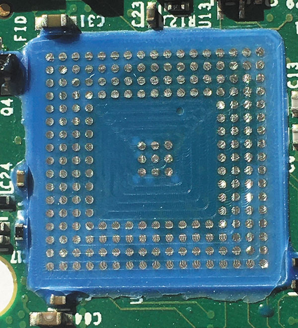
FIGURE 9. BGA removed using cold removal process.
The PCB component milling removal process has become more automated, and many previous shortcomings in milling of electronic components have been overcome. These process developments, due to the built-in vacuum chuck and real-time, high precision laser-guided depth measuring, make the latest commercial version of milling of components more attractive. The vibration as well as temperature effects of milling and resulting impact on solder joint reliability need further investigation to use this process on other assemblies. •
References
1. Syed Wasif Ali and Michael Yu, “Underfill Revisited: How a Decades-Old Technique Enables Smaller, More Durable PCBs,” Embedded.com, Jan. 27, 2011; https://www.embedded.com/underfill-revisited-how-a-decades-old-technique-enables-smaller-more-durable-pcbs.
2. iNEMI, 2019 Roadmap, rework section.
3. J. England, et al, “Development of an Underfill Rework Process and Evaluation of Underfill Reworkability,” Proceedings of SMTA International, 2014.
4. Brian Czaplicki, “Get Rid of the Wooden Pick and Other Neanderthal Approaches for Rework of Underfilled Components,” Proceedings of IPC Apex Expo, 2019.
5. F. Xie, et al, “WLCSP and BGA Reworkable Underfill Evaluation and Reliability,” Proceedings of SMTA International, 2015; https://studylib.net/doc/18279365/wlcsp-and-bga-reworkable-underfill-evaluation-and.
is president of Best, Inc. (solder.net); bwet@solder.net.


Press Releases
- XLR8 EMS Welcomes Raul Jorge Lopez Jr. as Director of Program Management and Procurement
- Koh Young America Promotes Ramiro Mora to Lead Service and Applications in Mexico and South America
- ViTrox Americas Welcomes Huy Pham as Technical Support Engineer
- XLR8 EMS Appoints Steve Dutton as Chief Sales Officer