Features Articles
Multiple ways to refine inventory management.
Implementing Lean manufacturing principles means figuring out the right tradeoffs. In a perfect world inventories arrive just-in-time from a small pool of suppliers that have agreed to work to a common forecasting and lot-size philosophy.
A look at piezoelectric-based pump technology for jetting materials in low volumes.
Requirements for higher speed and precision in applying very small volumes of material in precise locations have been met with the development of better pump technologies and dispense methodologies for a much more controlled and automated process with tighter tolerance levels and higher throughput. One such example is jetting technology. Jetting has been widely used since the 1990s to expel controlled amounts of material at low volumes. Jetting dispenses droplets of fluid from the nozzle tip and propagates them toward the target in precise volumes via the striking motion of a piston over a seat. Jetting replaced needle dispensing, which requires Z-axis motion to dispense good quality dots. Jetting, which does not require Z motion, is performed on the fly; i.e., dots are fired while the head is moving from one dispense location to another. Jetting technology is much faster than needle dispensing and produces more stable, controlled, and tinier deposits.
The newest pump technology to emerge for jetting is piezoelectric-based, capable of depositing materials in low volumes to much tighter tolerances. These pumps are able to control dot size and volume consistently; mass depositions down to 12 nanoliters with precise dot placement accuracy have been achieved. One such pump works on the principle of a closed loop control system along with two sensors to track the position of a piston and armature yoke which holds the piston during the upstroke, as well as the downstroke, motion. An adaptive feed forward control works to drive the upcoming stroke of the piston, this being dependent on the preceding strokes to maintain the required charge, measured by the output of an encoder with an incremental resolution of 25nm. The piezoelectric motion is amplified by a lever mechanism to provide the maximum charge of 0.5mm needed to dispense different dot sizes at desired frequencies. Piezo actuators also permit a rapid valve actuation, repeatable in nature, to control the amount of fluid jetted out of the orifice during one complete stroke. This offers the ability to control dot size, operation speed, and improve higher dot positional accuracy with better dot characteristics, e.g., good circularity.
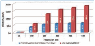
Faster dispensing. The blue column in Figure 1 illustrates a 65% reduction in cycle time operating at 500Hz versus 50Hz. A piezoelectric pump can operate at a high actuation frequency of 500Hz, providing a UPH advantage of 186% compared to a low frequency of 50Hz. Indicated UPH and cycle time percentages have been calculated by running a programmed test that includes lines and dot commands in the process program as were run in a production environment.

Figure 1. Improvement in throughput.
A frequency of 500Hz implies that the pump can dispense 500 shots per second on the substrate. Pump hardware configuration and characteristics of the dispense fluid can have a profound effect on droplet size and dispensing performance. For that reason, piezoelectric pump operation (which is complex) must rely on closed-loop control and powerful software tools that auto-tune the “charge,” which affects droplet size.
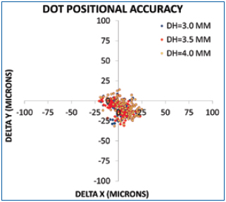
Dot positional accuracy. Dot positional accuracy is measured as the difference between the commanded position and the actual dispensed position for each individual dot through dispensing an array of dots. In multiple tests, dot positional accuracy test results are within ±25µm for Loctite Eccobond 3838T epoxy adhesive for different dispense heights varying from 3.0 to 4.0mm. Such good accuracy even at higher dispense height provides an advantage in the ability to dispense within tighter pitches between components. 
Figure 2. Dot positional accuracy at different dispense heights (DH).
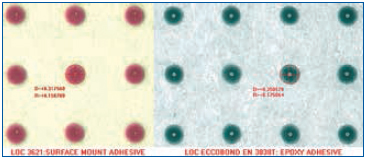
Dot footprint and circularity. Dot footprint defines how the dot gets placed on the substrate with good dot diameter accuracy and no contamination to adjacent components. Visual inspection shows good dot quality with good positional accuracy, even with dots close to 300µm in diameter, with no satellite formation. 
Figure 3. Dot footprints on copper pad.
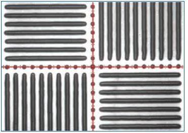
Line quality. Line quality depends on the dot characteristics in terms of dot positional accuracy and circularity. Line width is defined by the series of dots dispensed at a correct spacing to align properly to form a straight and non-scalloped line. Once the dots touch each other, the boundary is scalloped but the dots are compressed further, and fluid takes the shortest path to the deepest scallop to form a perfectly straight line. The closer the dispense head to the substrate, the better the line quality.

Figure 4. Line quality from dispense height of 3.5mm at line width of 3 dots per mm.
In summary, jetting has become a standard dispense method in assembly production. Real-time adaptive feed forward controls enable a more repeatable actuation of the jet, enabling higher repeatability at faster cycle rates. Jetting can be used with a variety of fluids for a range of applications in the PCB assembly, advanced semiconductor packaging, LED assembly, flat-panel display assembly, and electromechanical devices and products that support alternative energy resources.
Sunny Agarwal is applications engineer II at Speedline Technologies (speedlinetech.com); sagarwal@speedlinetech.com.

It depends not just on where one looks, but when.
Are these open connections, non-reflow or good quality control? It all depends on which stage of the process the product is in when inspected.
Parity emerges among EMS Factories from Asia, Mexico and the US.
For the first time in years we see parity in the Eastern US among EMS factories from Asia, Mexico and the US. This EMS market condition will permit American OEMs (the EMS industry refers to OEMs as customers) to have more EMS pathways to choose from. Now more than ever, such EMS assignments will require deeper investigation relating to the OEMs’ evaluation of manufacturing strategies.

Thin boards are prone to vacuum suction, increasing the risk of over-prints.
Despite the provocative headline, this column is not a rant about how much I despise defects or the havoc they wreak on yields and profits; that’s already well established! Rather, this month’s space will focus on dedicated tooling and print platform vacuum control.


