

Features Articles

Correlating inspection trending with test data to fine-tune accept/reject parameters.
Industry 4.0 automated inspection technology opens the door to enhanced levels of process control. In addition to having to upgrade equipment, however, fully leveraging the power of this technology requires a strong team, an accurate program validation database, and a methodology to track trends in continuous improvement activities. Here is a look at an implementation process for inline 3-D solder paste inspection and 3-D automated optical inspection following reflow on SigmaTron’s SMT lines in Tijuana.
A planned phase two of this implementation includes adding 3-D AOI to secondary assembly operations post-SMT, plus correlating AOI trending with final test data to fine-tune AOI acceptance/rejection parameters. The facility is currently averaging 50ppm defect rates across its SMT lines. The goal of this greater inspection process is to drop that to zero defects; although, given material constraints are driving a defective component rate that represents a third of that 50ppm level on some programs, zero ppms may be unachievable until material availability returns to normal.

Engineers know a snow job when they hear it.
Dear Mr. Christ,
Knowing you’re a busy man, we’ll cut to the chase: Our firm is offering you an exclusive list of the five million attendees to your recent motivational speech on the mountain. Our proprietary Digitaldisciple algorithms identify those most receptive to your message, broken down by district in Judea, so you can focus on the finer points of conversion, based on leaders and laggards, attendance-wise. We’ve done the work, so you don’t have to, for a very – dare we say it – revelatory price. Others promise salvation in the form of prescreened customer lists, but only we deliver. Accept no substitutes! Click the link at the bottom of this email, and a customer service representative will contact you soon about how we can make the Beatitudes work for you!
You know those lists? Of course you do.
They’re the ones whose salespersons relentlessly appeal to our inner greed, breathlessly promising delivery to the recipient of a complete roster of attendees to one’s favorite trade show. Or equipment users’ group. Or industry association annual meeting. All guaranteed.
The unspoken and alluring premise is a name on a list is simply a customer you have yet to contact. Who doesn’t want a new customer? Better yet, a complete list of vetted customers? These services furnish the list. All you have to do is follow up.
Their pitch probably lands in your inbox or spam folder regularly. For many, that means weekly. For a “privileged” cohort, daily. Usually deleted upon arrival. Too good to be true.
Is it?
Ever wonder how they work? I tried an experiment.
Beginning Feb. 7, 2022, and ending Jun. 10, 2022, I saved every email appeal for list services. In those 88 business days (no holidays included), 206 unsolicited pitches arrived in my inbox. That’s 2.34 per working day, a sample size sufficiently large to assess the range and depth of what is being offered.
So, what is being offered?
Not much range and very little depth.
Like this:
Hi,
I am following up to confirm you are interested in acquiring the Visitors/Registrants List.
Space Tech Expo
May 23-25, 2022
Long Beach Convention & Entertainment Center, Long Beach, USA
Registrant Counts: 4,280
Each record of the list contains: Contact Name, Email Address, Company Name, URL/Website, Phone No, Title/Designation
Seems tempting. But wait, there’s more:
I am following up to confirm if you are interested in acquiring the Visitors/Attendees List.
Space Tech Expo
May 23-25, 2022
Long Beach, California, USA
Registrant Counts: 10,000
Different ads on different days but almost the same script. Different company (allegedly), same speechwriter. Probably the output of one server in someone’s bedroom in a remote corner of Sumatra. Bigger registration count. One highlighted a battalion, the other a regiment. This is a business model with a decidedly dim view of human nature. Bigger numbers mean bigger appeal. Don’t forget that greed thing.
These are inflationary times, after all.
One of those 10,000 might hold the key to my retirement. (Then again, so would the lottery.) Except I have many other competing pitches for Space Tech, with projected quantities of attendees ranging all over the map: 2,000; 3,842; 11,000; 13,445; and 20,099. (Why didn’t they just round that last number up to 20,100? Does 20,099 somehow look more authentic?) The regiment has grown to a brigade, even a full division. Which to choose?
Another Space Tech cold email badgered me 26 times in a one-month span, gradually reducing its price as I remained nonresponsive, from a starting $800 to an ending $400. Endure an extra month of digital harassment, and, by projection, it should fall to the quite-affordable rate of zero.
Another sample from the inbox:
Dear Exhibitor,
I am following up to confirm if you are interested in acquiring the Attendee List.
Houston Expo & Tech Forum
Mar. 24, 2022
Stafford Centre, Stafford, USA
Counts: 2,560
Each Record of the Attendee Includes: Client Name, Business Name, Title, Email Address, Phone Number, Web Address, etc.
Let me know your thoughts, so I can send discount cost and additional information.
And this:
Hope you are doing well!
We are following up to see if you would be interested in the Attendee list of:
Houston Expo & Tech Forum
Date: Mar. 24, 2022
Stafford Centre, Stafford, USA
Are you interested in acquiring the Attendees’ info? (19,300+ Attendees)
Attendees’ information fields: Company Name, Company URL, Contact Names, Title, Phone Number, Email Address
Let me know your thoughts, so I can send the cost and additional information.
We have a Special 50% Discount offer for this month.
We are looking forward to hearing from you!
Six identical pitches, each requesting my thoughts (thank you very much), received on the same day, two each from three different companies. Supposedly. All of them equally wrong in their attendance projections. The 2022 SMTA Houston Expo and Tech Forum, held on one day, Mar. 24, had attendance considerably south of 19,300, a small city. Actual attendance resembled a small neighborhood.
Then there’s this:
Thank you for showing interest in our listings, and below are the details for list acquisition:
Project Details:
Show Name: Automotive Testing Expo Europe 2022
Total Counts: 20,000+ opt-in contacts
Discounted Price: €1,300
- Data Fields: Contact Name, Title, Phone Number, Fax Number, Physical address, State/City, Company Name, Company URL, and verified email addresses
- 90%+ accuracy and deliverability on all data fields
- Data will be provided in an Excel spreadsheet for unlimited list usage
- All the contacts are permission-based and authorized to receive the third-party information.
Let me know if you need more details, and I await your response. Thank you!
It’s reassuring the process is permission-based (what’s the alternative, coercion-based?) and that it’s 90% accurate (relative to what?). Pity the 10%, banished to Inaccuracy Purgatory.
Samples sampled randomly, and thus enticed, time to bite. So, I took the plunge and replied to a handful. The response was like blood sprinkled on a shark-strewn sea. Except some sharks are more discriminating than others.
For example, this is the five-figure approach:
- Target List of prospects based on your specifications (zip codes, counties, etc.)
- A fully managed multi-touch, multichannel lead management program
- Dedicated Sales Development Representative who will be making the calls
- Client Success Manager who will be your point of contact
- Quality Assurance Analyst to qualify every lead submitted meets your criteria
- Script, email templates, social and website marketing setup, which you will pre-approve prior to the start of the program
- Access to our web-based lead management platform, where you can monitor and organize, in real time, all the leads that have been qualified for you
I’m sure this is what Jeff Bezos and Elon Musk use every day before breakfast, once the rich zip codes are fully saturated with sales. A bit beyond my pay grade and budget, but nice to know this service is available once I make my first billion.
Back on Earth, here is the more prosaic, poor person’s approach:
It’s a half-price sale!
We are offering a 50% discount.
You can now acquire the info at $400.
Maybe they offer a payment plan.
Or there’s the middle-of-the road, semi-tailor-made approach, filling space with words, revealing little:
What we do for each client is customized, so it really depends on exactly what your objectives are. However, based on what your website says, I think we would probably look at our automated outbound systems to very targeted prospects that would be a good fit for your business, using our process of rapid sales communication testing, combined with your experience, to identify the best messages to communicate to your buyers. Ultimately our objective is to set up a steady flow of new high-quality sales meetings for you each month.
Let me know if that resonates with you, and we could look at trying to find a time for a quick chat.
Automated outbound systems?
Soundwaves generally resonate with me. Businesspeople have conversations. They don’t “chat.”
Here’s the thing: AI-inspired attendee databases are a mass-marketing approach that is unsuitable for small engineering businesses like ours. Our sales pitch is too technical. It can’t be faked. Engineers know a snow job when they hear it. Test parameters, specifications and detailed requirements like power-on testing, JTAG, 4-wire tests and 1149.1/1149.6 rules don’t lend themselves to a spreadsheet with 20,099 potential contacts. There may not have been that many JTAG users in the whole of human history. Nor does an x-ray inspection requirement stipulating resolution, focal length, scan energy, field of view, area of interest and desired pixel/voxel size find clear expression in a shotgun approach to marketing. At our level, one needs to listen to the customer. After listening and digesting the need, you either provide the service or you don’t. This includes supporting nontechnical customers who crave honest guidance on prudent use of their test dollars. A superficial, cold-calling approach to sales risks being more off-putting than enticing. Reputational risk is real. Our clients tend to have specific problems in need of very specific solutions. Test and inspection parameters, and their results, get scrutinized; often they’re second-guessed once the data are known. A high degree of customer contact and handholding is essential. One can’t afford to be dismissive or reluctant to explain (often repeatedly). Antagonize such prospects for any reason, and you’ll never hear from them again. Thank you, database and list folks, for your time, attention (a lot of that, once interest is shown) and education. Not now, but maybe in the future, as your systems get smarter, better defined and more focused. Obviously some small single-digit percentage of your cold calls succeeds; otherwise, I wouldn’t get 206 inquiries in 88 days. It’s just that you and my company aren’t a match. Yet.

Do all those spam emails offering huge contact lists that don't exist come from the same group?
Until then, the imagination still wanders and wonders:
Senator McCarthy, your recent speech in Wheeling, West Virginia, would have had a more accurate list of communists in government had you taken advantage of our Commienet services. Why be satisfied with only 205 names? For one low fee, our patented statistical analysis would have given you a list of 5,280 embedded subversives in the State Department and elsewhere in Washington. Consider the advantages of one-stop shopping and make technology your patriotic ally.
Mr. Haldeman, our Paranoiacom custom database will significantly expand your enemies list, virtually and literally, overnight. Why limit your outreach to The Washington Post and certain precincts in Manhattan? Data, like grudges, can be driven anywhere, and all the world’s fair game. Fortunately, for your sake, there’s us. Our firm provides the numbers – every name a prospective enemy – you can simmer over.
For us, refined application of the technology would appear to be in its infancy. Of such developments is progress made, knowing full well that infants’ adherence to a script is, well, unpredictable.
And the folks who offer the declining balance? (See above.) This morning they renewed acquaintances with yet another discount offer: 28 days left for no fee.
is president of Datest Corp. (datest.com); rboguski@datest.com. His column runs bimonthly.

Large crowds mulled the latest substrate trends and new developments in 3-D IC hybrid bonding.
The IEEE Electronics Components and Technology Conference (ECTC) returned to an in-person conference at the end of May with more than 1,500 attendees, domestic and international. Attendance in San Diego matched pre-pandemic numbers. While some presentations remained virtual, using video recording, many were onsite. A variety of electronics packaging topics were discussed. Judging by the crowded rooms, this year’s hot topic was 3-D IC hybrid bonding.
Advanced packaging. A pre-conference Heterogeneous Integration Roadmap workshop discussed trends in networking for the future and new developments in advanced packaging for high-performance computing and data centers. The workshop concluded with a panel of presenters discussing the latest trends in medical health and wearables.
Plenary sessions covered some of the latest topics. The MicroLED display session focused on high-volume manufacturing progress and challenges. In a session on the evolution of IC substrate technology, panelists from Intel, Amkor, Ajinomoto, AT&S and Atotech discussed the latest substrate trends.
The special session – Meeting Next Generation Packaging Challenges from Chiplets to Co-packaged Optics – included panelists from AMD, Cisco, Marvell and Synopsys (FIGURE 1). Panelists discussed the importance of co-design and changing the approach to design, including system-level design. The combination of digital and photonics is coming. Integrating this in 3-D will include the laser, modulator, filters and detectors. Interfaces and the design platform are important for robust manufacturing, including product quality, debug and traceability, and in-field optimization. The panel concluded that, with increased use of chiplets, continued work is required in the areas of test and known good die (KGD), thermals, power deliver and system-level integrity. Adoption of standards such as the recently introduced UCIe is important to align the industry around an open platform to enable chiplet-based solutions. Thermal management remains one of the major bottlenecks with 3-D.
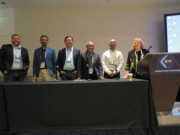
FIGURE 1. A special panel on packaging challenges. Panelists included (from left) Kevin O’Buckley (Marvell), Raja Swaminathan (AMD), Ming Zhang (Synopsys), Ravi Mahajan (Intel), Sandeep Razdan (Cisco Systems), and moderator Jan Vardaman (TechSearch).
A special night session focused on the US Department of Defense (DoD) in the state-of-the-art heterogeneous integration (SHIP) program. The opening statement from the office of the Undersecretary of Defense for Research and Engineering explained the backdrop of the program. Speakers from Intel and Qorvo, recipients of US government funding, described their activities. Qorvo is focused on RF, and Intel is focused on high-performance computing with its embedded multi-die bridge (EMIB) technology. The panel admitted that, in the absence of a volume supplier of buildup substrates, the DoD depends on a global substrate procurement strategy.
A session on diversity and career growth provided advice from a panel of experts, including representatives from IBM, Lam Research, Edwards and Cadence. The plenary session covered digital transformation with participation from Intel, TSMC, Yole, Onto Innovation and Samsung. A late-night session focused on Interconnect Technologies for Chiplets with participants from Intel, IBM, Unimicron, TSMC, SPIL and Furukawa Electric. Participants from Taiwan and Japan dialed into the session to discuss topics including embedded bridge, the incorporation of memory in advanced package developments in optical packaging, 3-D packaging and substrates.
Adapting to substrate shortages. With the continued substrate shortage, companies focused on the potential for a fan-out wafer level package (FO-WLP). Numerous presentations covered several options, with new applications for fan-out discussed. SK Hynix discussed the potential for memory applications. IME A*Star discussed FO-WLP antenna-in-package (AiP) for automotive radar applications. Researchers at UCLA described their work on FO for micro displays. RFcore discussed FO-AiP for 5G mmWave applications. Amkor, ASE and Samsung presented package options for FO-WLP.
Processing FO in a panel has been proposed as a way to lower the cost by increasing the number of parts with large-area processing. Fraunhofer and the Technical University of Berlin discussed the technology limits of panel processing, describing warpage and die shift as the major issues. Layout adaptation is promoted to overcome die-shift challenges on large panels. Samsung Electronics discussed the reliability of the via structure in its FOPLP line. Amkor introduced its 650mm x 650mm panel line. Nepes provided reliability data on FO packages fabricated on its new panel line based on Deca M-Series technology (FIGURE 2). Deca Technologies described 20µm device pad pitch with its M-Series process. The use of adaptive patterning provides a way to handle die shift. Dai Nippon Printing introduced its panel-based RDL interposer with a 2µm pitch semi-adaptive process for chiplet integration.

FIGURE 2. The Nepes nPLP 600mm x 600mm fanout panel line reportedly can produce five times as many chips as one 300mm round panel.
Several presentations focused on new substrate options, including glass as a substrate and RDL interposers. Developments in glass substrates were introduced with papers from Korea Electronics Technology Institute and Georgia Tech. TSMC introduced its organic interposer CoWoS-R+ technology that replaces the silicon interposer with an RDL structure. The plus indicates the integration of a large amount of high-density integrated passive devices (IPDs) that serve as decoupling capacitors. The integrated de-cap capacitors suppress the power domain noise and enhance HBM3 signal integrity at a high data rate. Optional silicon connection blocks (bridges) provide high-density die-to-die connections. IBM provided updated work on its direct bonded heterogeneous integration (DBHi) silicon-bridge package, in which the Si bridge is connected to the die and then mounted on the laminate substrate. SPIL provided recent reliability data for its embedded bridge package. Unimicron discussed its hybrid substrate with a buildup film.
3-D hybrid bonding. Three years ago, many ECTC papers focused on R&D activities in hybrid bonding. This year, more than 30 papers discussed hybrid bonding process improvements and new developments. While image sensors have been using hybrid bonding for many years, Sony described their recent work to develop 1µm face-to-face bonding and a new thinning process that minimizes Si thickness variation across the wafer. Adeia’s (formerly Xperi) study of the influence of Cu microstructure on the thermal budget shows the possibility of a 20° to 40° reduction in the final anneal temperature. CEA-Leti presented research conducted with Intel on a new die-to-wafer (D2W) collective bonding self-assembly process using water droplets with high alignment accuracy and high throughput. SK Hynix reported the work on wafer-to-wafer (W2S) DRAM stacking for DRAM. Samsung presented several papers on hybrid bonding, including research on controlling bonding voids. AMD described its V-Cache, now in commercial production for servers, desktops and gaming, using TSMC’s SoIC process. TSMC described an extension of its SoIC process.
Co-packaged optics. Several presentations focused on co-packaged optics (CPO). Rockley Photonics introduced a fan-out silicon photonics module for next-generation CPO. Rain Tree and IME A*STAR described a heterogeneous integration package using FO-WLP for a hyperscale data center. IBM Canada, GlobalFoundries and others discussed optical fiber pigtail integration for CPO. Cisco described its vision for CPO and challenges in the use of through-silicon vias, including high warpage, optical fiber coupling, and chip-on-substrate assembly. Reliability requirements were also highlighted. A joint paper from EV Group, Tyndall National Institute, IMEC and Ghent University described a high-speed Si photonic switch with a micro-transfer-printed III-V amplifier. ASE described its CPO assembly.
Emerging areas. Presentations also covered additive manufacturing, 3-D printing, developments in packaging and assembly for wearables, and micro LEDs.
Next year’s ECTC will be held in Orlando May 30 to Jun. 2.
is president of TechSearch International (techsearchinc.com); jan@techsearchinc.com.

Limiting PCB moisture absorption is the full responsibility of the supplier. How to pack boards right.
PCB suppliers who use good packaging methods are keeping their products safe from physical damage incurred during transit from the manufacturing facility to customers’ warehouses. Equally important, these packaging practices help ensure shelf-life expectancy by preventing moisture absorption.
To protect their orders, PCB buyers should require suppliers strictly follow corporate shipping specifications. Nothing is more frustrating than waiting for quality product to be built, only to have it damaged because of poor packaging practices. It’s just as frustrating when boards become useless while sitting on the shelf.
PCBs can be very heavy. Their sharp corners sometimes wreak havoc on the corrugated cardboard boxes in which they are shipped. A good freight spec should state boards are to be vacuum-packed with a bubble wrap base, with no more than 25 boards to a stack. When a board is oversized or heavier than normal, 10 to 15 pieces is the best option. Whatever number is used, the packaging should be consistent in count for a particular shipment.
Extra care should be taken for flexible or very thin, rigid PCBs less than 0.028" thick. They should be packaged with stiffening material on the top and bottom of the bundle to help prevent warping.
A humidity indication card (HIC) and desiccant are to be placed within the package as well. The HIC should be placed inside on top of the PCBs for easy review. The desiccant should be placed along the side or edge of the bundle, so it doesn’t contribute to bending or warping caused by the stress of the vacuum packaging.
Each PCB bundle should have a sticker affixed detailing the part number, date code and number of pieces per bundle. More than one date code of the same product may be shipped together if they are segregated and marked as such.
X’d-out panels, if allowed by your PCB fabrication specifications, should be packaged separately and clearly marked.
The individual packages of PCBs should be placed tightly in a box, with Styrofoam or other shock- absorbing material placed between the packages and the wall of the shipping container. The PCB corners should be protected, as they can be easily dinged or dented while in transit.
The weight of each box should not exceed 30 lb. Boxes may have exterior strapping applied when the PCBs are oversized or heavier than normal.
Each box should have a sticker on either end identifying its contents, including the part number, purchase order number, date code and number of pieces within the box.
Each part number shipped should come with a packing slip and “proof of quality” documentation, including (but not be limited to):
- The certificate of compliance
- A first article or dimensional report
- A microsection report to include a solderability test with a cross-section
- An electrical test report
- An ionic contamination report
- A TDR report (controlled impedance, when applicable)
- Any material certifications
- Any other documentation required by the purchase order.
When the product is shipped, the supplier should notify the customer’s purchasing, receiving and accounting departments of shipment method and tracking number. The commercial invoice and electronic copies of the quality paperwork should be included in case such documentation for the shipment is lost in transit.
As crucial as proper PCB packaging is, the storage of the boards once they reach the customer is just as vital. Other than opening one of the packages to verify the PCBs meet the criteria of the print and the documentation received, the best bet is to leave the boards in their original packaging.
A bare board begins to absorb moisture immediately upon leaving the factory. The amount of moisture absorbed depends on a variety of factors, including:
- Base material used in manufacturing
- Manufacturing environment
- Packaging method
- Shipping temperatures (from the cold bellies of aircraft or the humid transit of a sea shipment to hot delivery trucks)
- Customer storage and inventory procedures.
Vacuum sealing and the use of desiccant only delay or lessen moisture absorption. They do not prevent it.
The longer a PCB is stored on a shelf, the greater the chance it will absorb moisture, which can manifest in the assembly operation as delamination. Delamination is caused either by moisture or manufacturing defects. If a problem PCB is determined to be structurally sound, the cause most likely is moisture-related. A bake-out process before any additional assembly can remove most of the moisture, if not all of it. This permits the board to be assembled without issue.
IPC-1602, Standard for Printed Board Handling and Storage, provides suggestions for proper handling, packaging and storage of PCBs. It puts the full responsibility for PCB moisture content on the supplier, even after the finished product has left the manufacturing facility.
The way PCB suppliers package their products indicates their commitment to quality and reliability. It is the final step in the manufacturing process, and PCB buyers have a responsibility to ensure it is done right.
has more than 25 years’ experience selling PCBs directly for various fabricators and as founder of a leading distributor. He is cofounder of Better Board Buying (boardbuying.com); greg@directpcb.com.

Fabricators and designers must communicate about new technology to verify its viability.
More often than not over the past couple of decades, new technologies, processes and options we fabricators have been asked, begged or threatened to add to our repertoire of offerings were ones that could be best considered disruptive. What’s disruptive to a manufacturer may seem benign to the casual eye, as often the technology – or process – that is most disruptive is a simple one.
Indeed, sometimes that technology is nothing more than the rebirth of an older, tried-and-true, albeit significantly tweaked, process. REACH, and the prior RoHS, caused much disruption, and yet most of the plating chemistries and surface finishes in use today are essentially highly refined formulas of older plating technologies such as ENIG, silver and tin.
Old or new, disruptive technologies tend to be challenges for several reasons. First is understanding the technology and how to process it so it works as intended. Second is determining what equipment is needed to cost-effectively and robustly apply the new technology. Finally, finding enough customers to consistently order product that uses the technology, so everyone remembers what it is and how to process it!
Truly new paradigm-shifting technologies hit the scene as “must haves” so a product can function. While disruptive to manufacturers, in some ways the more off-the-wall a technology seems, the easier it is to decide whether to embrace it or wait to see if it sinks under the weight of its own hype. These disruptive technologies more typically challenge everyone to understand not only how to apply them, but how to measure success or failure so yields and costs can be determined.
In all cases, what makes disruptive technologies so unruly boils down to two issues: First is the learning curve and capital investment needed to provide the technology, and second is gaining consensus among customers that the technology is a better alternative to more traditional technologies, and they will purchase enough to warrant the human and capital investment. Probably most frustrating for fabricators is when a buyer provides no apparent reason other than “because” for specifying a new technology. The fabricator’s goal is to supply quality product they understand and can safely and consistently produce, not (inadvertently) become a customer’s R&D center, with the concurrent risks and costs.
Every new technology has at least two sides. At a recent industry gathering, a supplier mentioned a current disruptive technology we had difficulty working our way through was only one of a slew of new “enabling” technologies available to the industry. Enabling? Not to me. That is when the communication gap between design application and manufacturing competence became evident. As this conversation continued, I heard a different spin as to why a particular new technology was being specified. Understanding the benefits from the end-product perspective began to make sense and explained why this customer would have specified it, as well as why its use may become widespread in the future. The tutorial was strictly from a value-add design perspective, and it was compelling. When asked if the design community knew of the fabrication challenges the new technology caused that impacted yield and lead times, in addition to cost, the answer was honest: “Probably not.”
What’s enabling to one party can be disruptive to another. Fabricators often do not understand the nuances of pushing design to meet challenging performance objectives but do fully understand robust, time-proven manufacturing techniques. Equally, when a designer chooses to move toward a new technology, they may be excited by the functionality it offers but most likely is unaware manufacturing the board could lead to lower yield, longer lead times and ultimately higher costs.
The real issue is understanding the risks involved with embracing – or ignoring – new technology. The risks include, “Will it work, or will it only work if executed flawlessly? Will the new technology pass the test of time? Most important, will widespread use of the technology lead to cost-effective processes or equipment to ensure consistency from one application to another and from one supplier to another?”
As a fabricator, it is more important now than ever to be in touch with customers’ designers to understand what they are attempting to accomplish. Equally for designers, it is essential they are in contact with all their PCB suppliers, especially the behind-the-scenes process gurus, so everyone understands the manufacturability of new technology in the real world of the shop floor.
This gets back to the need for suppliers knowing their customer and customers knowing their suppliers – and not just at the buyer/sales rep level but at the designer/manufacturing engineer level. Knowing the intended end-result a new technology enables, as well as how disruptive that technology may be when introduced to manufacturing, the product is the best way for customers and suppliers, working together, to accomplish a cost-effective design. Too often this communication is wrongly assumed to occur. As much as frequent two-way communication should be happening when all is moving along with traditional technologies, it is critical the communication takes place when a new approach is contemplated that may be enabling for one but not necessarily for others.
The difference as to whether a technology is enabling or disruptive is determined only by the degree in which customer and supplier decide to work together. As our industry finds ways to tweak older, reliable technologies or develop paradigm-changing ones, understanding the enabling benefits and the disruptive nature will make the journey mutually rewarding.
is president and CEO of IMI Inc.; pbigelow@imipcb.com. His column appears monthly.

The current difficulties call for a more strategic approach to arranging our global supply chains.
The supply chain chaos in the aftermath of the pandemic has highlighted the risks associated with globalization. As a phenomenon, globalization has served many of us well. Its ideological opponents, however, see today’s situation as justification for its demise. There is no denying current events have highlighted shortcomings. We would be foolish not to learn and adapt.
I’ve addressed the subject of onshoring as a potential antidote to globalization many times in the past. Arguably, now, the idea makes more sense than ever. On the face of it, shorter supply chains promise some protection against the unpredictability of today’s world. Hot on the heels of the pandemic, we now have the Ukraine crisis, and there is the fallout from Brexit, which has made for difficult and time-consuming trade between the region’s most influential economies. One major obstacle to the return of onshoring is essential indigenous-supporting industries have been largely swept away as activities have migrated offshore, taking expertise and investment with them. The conditions that caused and drove the offshoring remain in place, perhaps masked by current logistical difficulties. Accessing the data needed to move manufacturing activities from an established location is another barrier to reshoring.

Press Releases
- XLR8 EMS Welcomes Raul Jorge Lopez Jr. as Director of Program Management and Procurement
- Koh Young America Promotes Ramiro Mora to Lead Service and Applications in Mexico and South America
- ViTrox Americas Welcomes Huy Pham as Technical Support Engineer
- XLR8 EMS Appoints Steve Dutton as Chief Sales Officer