

Rework of New High-Speed Press-Fit Connectors
An in-depth study shows connection strength is most affected by the size, material and geometries of the press-fit pins, hole sizes and hole plating.
This article has its roots in the need to perform multiple reworks of an early version of a new family of high-speed press-fit connectors with a sensitive mechanical buildup. The challenge has been to press in the thin and weak needle eye pins correctly. Different variants of this press-fit connector, with slightly different pin geometries and materials, were shown to cause damage of different kinds in the plated holes during rework. After several redesigns, this specific high-speed press-fit connector became more robust, but the need to find out more about the effects of rework for this type of connector remained.
With several other high-speed press-fit connectors about to be introduced, there is a general need to evaluate the damage multiple reworks could cause. Almost no information about rework of these new press-fit connectors has been published, which increased the necessity of this investigation. FIGURE 1 shows an example of deformed high-speed connector press-fit pins inserted in plated holes of different sizes. The goal of this project was to understand how rework of these new high-speed press-fit connectors affects connection strengths, hole wall deformations and plating cracks.
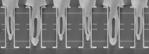
Figure 1. A 3D CT x-ray image of deformed high-speed press fit connection pins.
Methodology
This evaluation included rework from zero up to three times of a selected group of new high-speed connectors on test boards with different hole plating and hole sizes covering the complete hole diameter tolerance range for each connector.
After rework, three different evaluations were performed:
- Single pin insertion and retention strength test. The forces to press in and to pull out single pins from each of the tested connectors were measured to determine whether the connection strengths had been affected by the rework.
- Gas tightness test. By measuring electrical resistance between plated hole walls and press-fit pins before and after subjecting assemblies to aggressive gas, possible hole wall cracks or general bad connections between pins and hole walls could be detected. Hole wall plating cracks would mean corrosion took place during the storage in aggressive gases, and this would increase the electrical resistance.
- Cross-sectioning. To better understand results from the insertion, retention and the gas tightness tests, precision cross-sections of the holes with connector pins have been performed. Hole wall deformation and other board damages were studied, as was the shape of the needle eye pins in the holes.
Test Materials
Connectors and test boards used in this study are described below.
New high-speed press-fit connectors. Four new high-speed connectors, named A, B, C and E, were chosen for this rework evaluation. One old connector, named D, which is not considered high-speed, was used as a reference. To better understand the results from the rework tests, thorough pin measurements were performed for each of the connectors.
High-speed press-fit connector A had slightly bigger pins than the other tested connectors. The recommended board hole diameter was 0.46mm ±0.05mm, both for the ground pins and for the signal pins. FIGURE 2 shows the bottom side of the package showing the compliant press-fit pins. Every third pin is a ground pin, and the shapes and sizes between the signal pins and ground pins differ. Measurements of the signal pins for connector A are shown in FIGURE 3. Measurements of ground pins for connector A are in FIGURE 4.
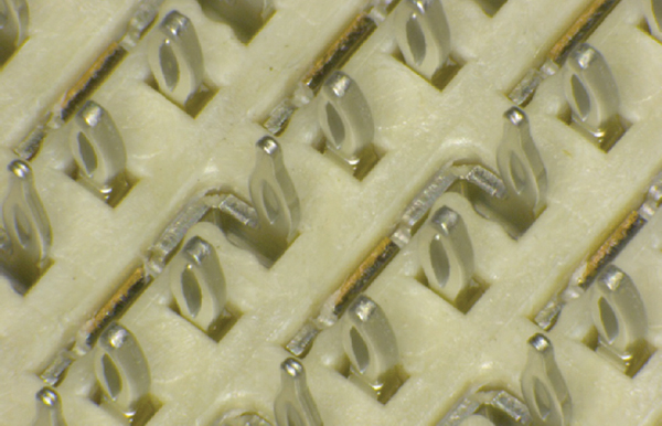
Figure 2. Press-fit pins for high-speed connector A.
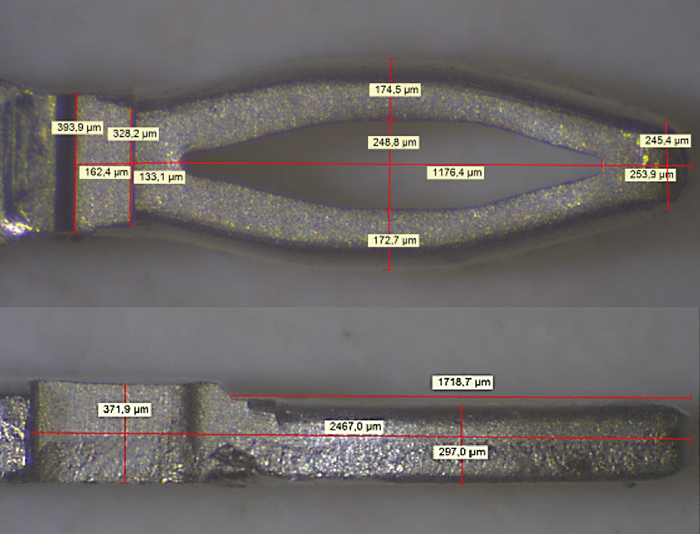
Figure 3. Press-fit signal pins for high-speed connector A.
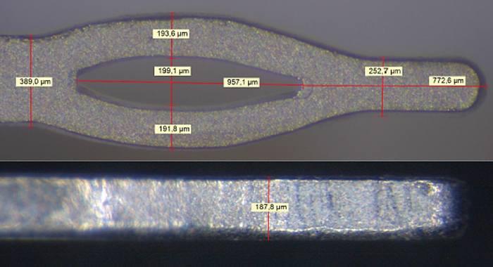
Figure 4. Press-fit ground pins for high-speed connector A.
Figures 3 and 4 show the signal pin material is thicker than the ground pin material. On the other hand, the needle eye opening is bigger for the signal pin than for the ground pin. The signal pin edges are more rounded than the edges for the ground pins. The pins consist of a bronze alloy plated with tin over nickel.
High-speed press-fit connector B has small signal pins made for 0.36mm ±0.05mm final hole diameters. The ground pins for this connector are much bigger than the signal pins and were not included in this evaluation.
FIGURE 5 shows the bottom side of the package showing the compliant press-fit pins. Every third pin is a ground pin, and the sizes and shapes differ very much between the ground pins and the signal pins.
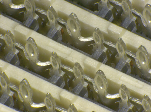
Figure 5. Press-fit pins for high-speed connector B.
FIGURE 6 shows the needle eye opening on the signal pins for connector B is rather big, and the sides of the needle eye are thin. The pins consist of copper plated with matte tin over nickel.
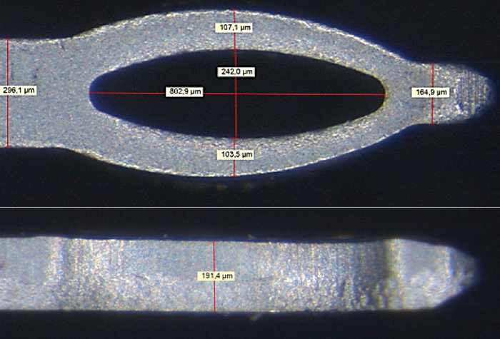
Figure 6. Press-fit signal pins for high-speed connector B.
High-speed press-fit connector C has small signal and ground pins aimed for 0.36mm ±0.05mm final hole diameters. The ground pins and signal pins have similar size and shape.
FIGURE 7 shows the bottom side of the package showing the compliant press-fit pins. The ground and signal pins are turned 90° relative to each other. Measurements of the signal pins for connector C are shown in FIGURE 8. The needle eye is slightly smaller in length and width than the other components’ pins, and the material on the sides of the needle eye is also thin. The pins are made of copper plated with nickel.
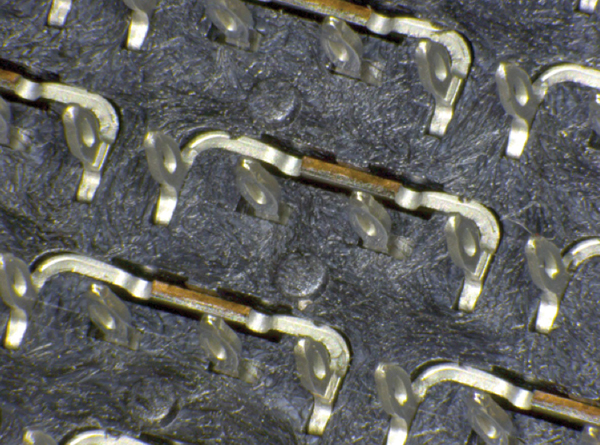
Figure 7. Press-fit pins for high-speed connector C.
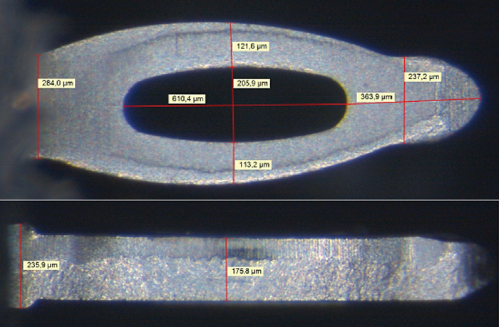
Figure 8. Press-fit signal pins for high-speed connector C.
The reference component is an old variant of a press-fit connector that does not use needle eye pins. Instead, the pins consist of a solid tip followed by a thin metal foil that conforms to the hole wall when inserted. The pins on the reference connector D are much bigger than the new high-speed connector pins evaluated in this study. Recommended final hole diameters for these pins are 1.00mm -0.0/+0.1mm. FIGURE 9 shows the bottom side of the package showing the compliant press-fit pins. FIGURE 10 shows measurements of a compliant pin from reference connector D. FIGURE 11 shows measurements of the solid tip of a press-fit pin for the reference connector D.
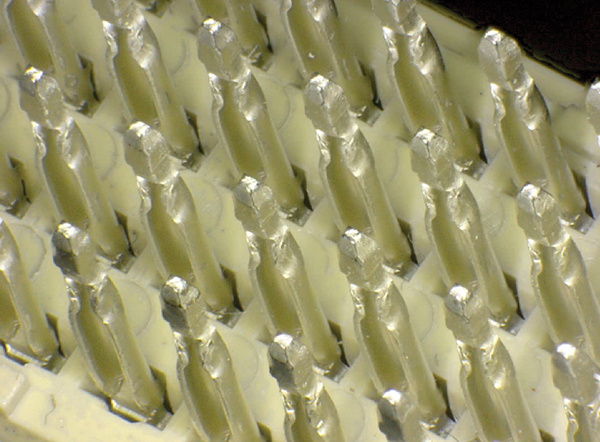
Figure 9. Press-fit pins for reference connector D.
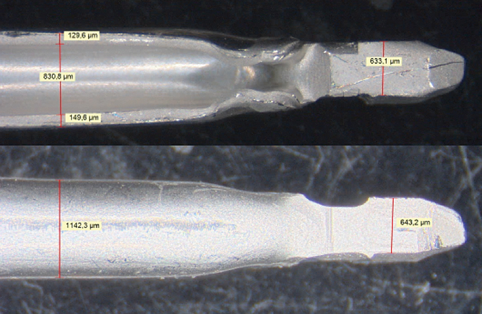
Figure 10. Measurements of press-fit pin for reference connector D.
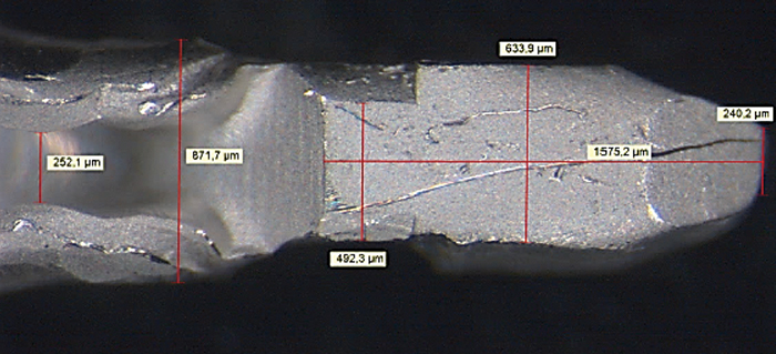
Figure 11. Measurements of press-fit pin for reference connector D.
As mentioned, the compliant pins for reference connector D are much bigger than the new high-speed press-fit connector pins, and the connection technology differs as well. Therefore, it is difficult to make fully justified comparisons between the reference connector and the other tested connectors. The pins consist of a bronze alloy plated with nickel.
High-speed press-fit connector E has small signal and ground pins aimed for 0.36±0.05mm final hole diameters. The ground pins and signal pins have similar size and shape. FIGURE 12 shows the bottom side of the package showing the compliant press-fit pins. The ground pins and signal pins form a rather complicated pin pattern, and they have slightly different geometries. FIGURE 13 shows measurements of signal pins for connector E, and FIGURE 14 shows measurements of ground pins for connector E.
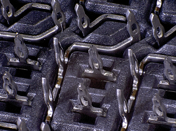
Figure 12. Press-fit pins for high-speed connector E.
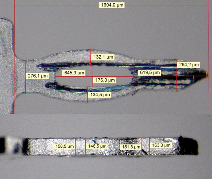
Figure 13. Press-fit signal pins for high-speed connector E.
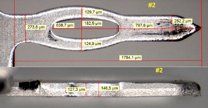
Figure 14. Press-fit ground pins for high-speed connector E.
Figure 13 shows the needle eye opening in the signal pins for connector E is rather small, and the sides of the needle eye are thick. The ground pins have slightly bigger needle eyes and thinner material at each eye side, which makes the insertion force lower. The pins’ base material is copper plated with matte tin over nickel.
TABLE 1 summarizes compliant pin measurements. In this study, only signal pins were used for insertion and retention tests. For the gas tightness test and cross-sectioning, signal and ground pins for connectors A, C and E have been included.
Table 1. Test Connector Pin Measurements – Summary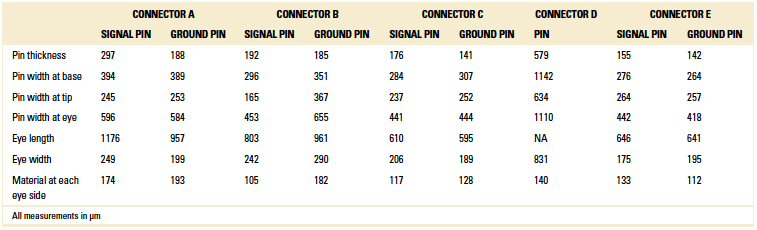
A special test board was designed for this press-fit rework evaluation. It was decided the final hole sizes should include each connector’s specified minimum, nominal and maximum diameters. These different hole sizes were made at each connector site.
FIGURE 15 shows a test board with ImSn hole plating and a test board with ENIG hole plating. Most of the design parameters for the test board were chosen to resemble those of a common base station or core network board. The board size was, however, much smaller in order for the board to fit into a gas tightness test chamber. The number of layers was also fewer than in an ordinary base station or core network board.
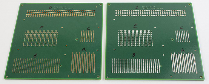
Figure 15. Test boards – ENIG (left), ImSn (right). The different component sites are marked A to E.
TABLE 2 lists board parameters.
Table 2. Test Board Parameters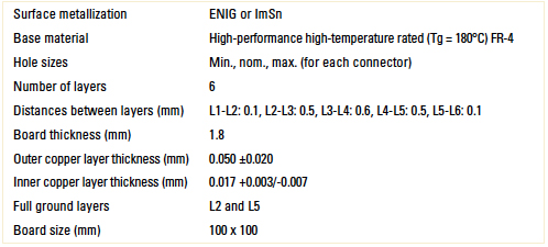
The most difficult part to succeed in when manufacturing the test boards was to receive the specified minimum, nominal and maximum final hole diameters for each of the tested high-speed press-fit connectors. The specified final hole dimensions for the test pins for each of the connectors are in TABLE 3.
Table 3. Final Hole Dimensions, Test Pins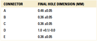
To receive the correct minimum, nominal and maximum final hole size for each of the tested new high-speed press-fit connectors, the drill sizes shown in TABLE 4 were used during the fabrication of the test boards. (Drill sizes were suggested by David Wice of Ciena.)
Table 4. Drill Sizes for the Different Sites on Test Board
After the test boards had been produced, the final hole diameters were measured, and one ImSn board and one ENIG board were cross-sectioned to verify dimensions.
FIGURE 16 shows an example from a test board cross-section of an ENIG plated hole intended for connector A. FIGURE 17 shows an example from a test board cross-section of an ImSn-plated hole intended for connector A. The cross-sectioning of two test boards (one ImSn and one ENIG) showed they had been well fabricated. No test board failures could be found.
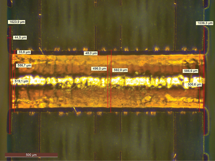
Figure 16. Cross-sectioning – ENIG board with hole for connector A.
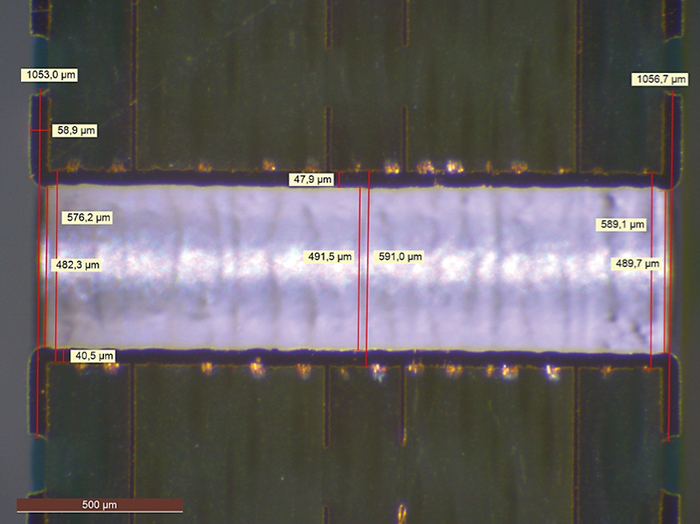
Figure 17. Cross-sectioning – ImSn board with hole for connector A.
The holes were also measured using an optical measurement machine (FIGURE 18). TABLES 5 and 6 show measurements of the hole diameters. The hole measurements show the ImSn-plated holes have slightly smaller diameters compared to the ENIG holes. One observation is both the minimum and maximum hole sizes have margins to the real specified limits. Another observation is the drill for connector A’s minimum hole was so close to the nominal hole drill that the final hole diameters’ difference is negligible for these holes.
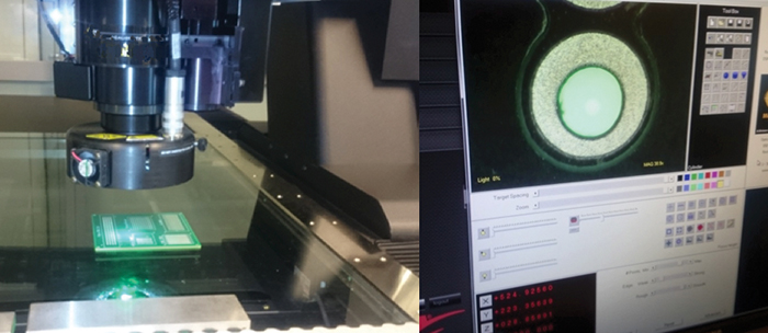
Figure 18. Optical hole diameter measurements.
Table 5. Measured Hole Diameters, ENIG Test Board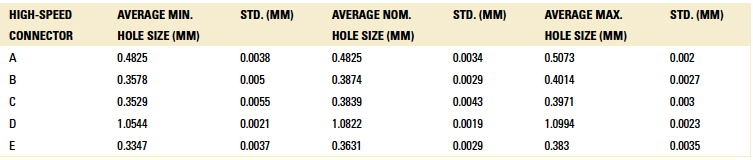
Table 6. Measured Hole Diameters, ImSn Test Board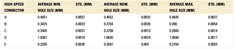
Apart from optical measurements, pin gauges were also for verification. A 0.45mm diameter pin gauge could, for example, fit in all tested minimum and nominal holes for connector A, while a 0.50mm diameter pin gauge could not fit. The standard deviations from the hole measurements are low, so there are indeed three different hole sizes for each of the connector sites, except for connector A, where there only are two.
As mentioned, minimum, nominal and maximum hole diameters were designed for each connector site. FIGURES 19 and 20 show drawings of the hole patterns where the minimum holes are red, the nominal holes green and the maximum holes yellow (except for connector site B, where the colors are light green for the minimum holes, blue for nominal and lilac for the maximum hole size. The red, green and yellow holes for connector B are big ground pinholes that all have the same diameter on this test board.)
Figure 19. Test board hole patterns for the connectors A (upper left), C (upper right), D (middle) and E (bottom).
Figure 20. Test board hole patterns for connector B.
The test boards were judged as well-manufactured and suitable for the press-fit rework evaluation.
Press-fit Rework
The demands and needs for removal and installation of each of the connectors were collected, and when all instructions and tools had arrived, the rework was performed.
Adapted tooling for pressing in the different connectors into the board was needed. FIGURE 21 shows examples of press-in tooling. One semiautomatic press-in machine was used in rework tests of connectors A and D, and another semiautomatic press-in machine was used for rework tests of connectors B and C. In both instances, the press-in speed could be programmed, and force was measured during the entire press-in process.
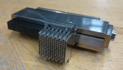
 Figure 21. Press in tooling intended for connector A (left), B (middle) and C (right).
FIGURE 22 shows one of the semiautomatic press-in machines while it is inserting connector B into one of the test boards. This machine was used to press-in connectors B and C.
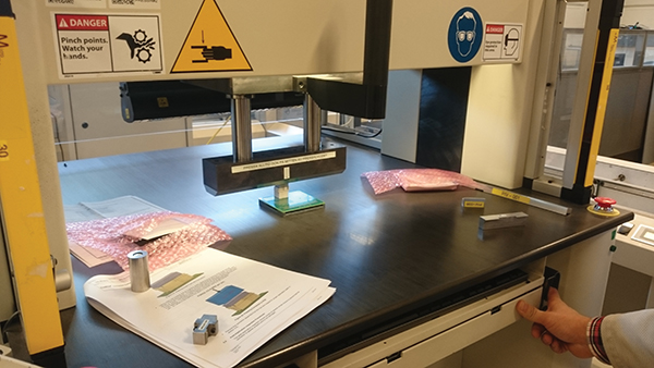
Figure 22. Press in of connector B during rework test.
The insertion force was measured during the press-in process for each of the connectors to ensure the maximum specified force was not exceeded for any of connectors A to D. Examples of typical force graphs are shown in FIGURE 23. A similar variant of press-in equipment as for connector B and C was used to press in the connectors A and D (FIGURE 24).
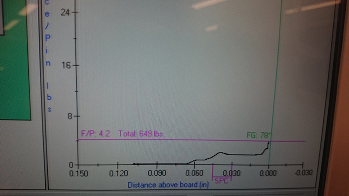
Figure 23. Press in force graphs for connector B (top) and C (bottom).
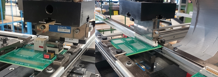
Figure 24. Press in of connector A (left) and D (right) during the rework test.
A typical graph from the press-in of the high-speed connector A is shown in FIGURE 25.
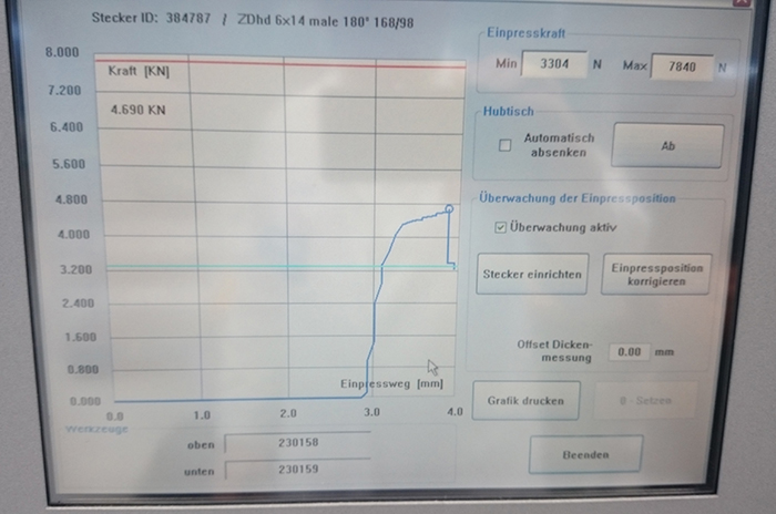
Figure 25. Press in force graph for connector A.
Connector E was reworked after the other four connectors and, at the time of this rework, no semiautomatic press-in machine was available. Because of this, manual press-in equipment was used. However, this machine was sensitive and of good quality, which made it possible to press-in the connectors smoothly and in a well-controlled manner.
In summary, the press-in processes succeeded to press-in the test connectors with the specified forces and times stated by the connector vendors.
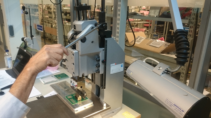
Figure 26. Manual press in of connector E.
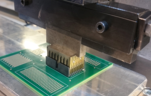
Figure 27. Press in of connector E during the rework test.
Removal. Instructions, tooling and processes for removing the connectors recommended by the connector manufacturers were used during all the removals, except for high-speed connector A because the specially adapted tool had not arrived in time for the test. Descriptions of the rework for each of the connectors follow.
Removal of connector A could not be performed with the specially adapted tooling, with small pins aimed at pushing out the needle eye press-fit connection pins, as was first planned. This tooling was not available at the time for the test. After consultation with the manufacturer of connector A, it was decided to use a thin manual tool, resembling a bent screwdriver, to break up the press-fit connections instead. The edge of the tool was placed under the outer part of the connector body and the package lifted by smoothly bending the tool. The tool was moved around all the package sides during the removal process. FIGURE 28 shows the removal of connector A.
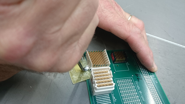
Figure 28. Removal of connector A.
The plated holes were inspected after the removal, and some holes had, unfortunately, been visibly damaged during the removal process. These holes were situated at the outer hole-rows. However, the inner-row holes and most of the holes in the periphery seemed undamaged.
For the removal of connector B, a specially adapted tooling was used with multiple thin pins made to push the press-fit pins out of the holes from below. In the first trials, the force needed to press out the connector was so high that the board bent too much. To avoid this, another test round was performed where a board support was used. This made it possible to remove the connector without bending the board. FIGURE 29 shows the removal process of connector B. The removal process for connector B, following the manufacturer’s recommendations, functioned very well.
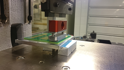
Figure 29. Removal of connector B with specially adapted tooling and board support.
The recommended method to remove connector C was to remove pin after pin and shield after shield with a pair of tweezers. This was performed without much effort. FIGURE 30 shows photos from the removal of connector C. Everything worked out well during the removal of connector C.
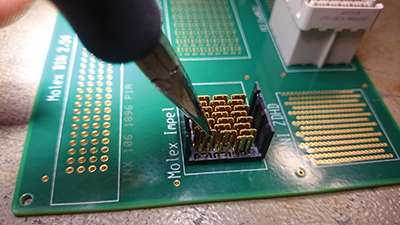
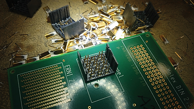
Figure 30. Removal of connector C.
For reference connector D, a flat rock tool was sufficient to remove the connector. This was the only one of the tested connectors with leads that protruded on the secondary side, so it was easy to use the tips of the pins to push them out from the holes. FIGURE 31 shows the removal of connector D. Everything worked perfectly well when removing the reference connector D.
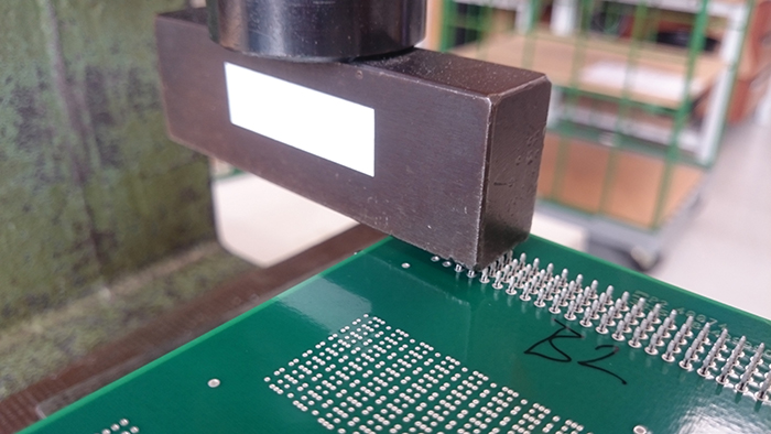
Figure 31. Removal of connector D.
For the removal of connector E, special tooling was used. The removal tooling consisted of five parts that needed to be assembled on and around the connector to be removed. The tooling was designed so that one part of it grasps under the edges of the bottom part of the connector body and lifts the connector when turning a screw knob. FIGURE 32 shows different parts of the removal tooling for connector E. A connector that is about to be removed is shown in FIGURE 33.
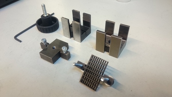
Figure 32. Tooling for removal of connector E.
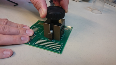
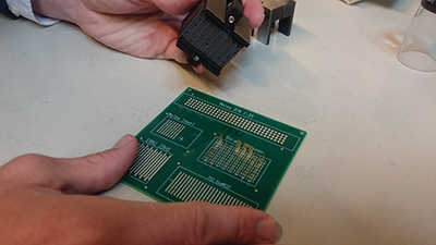
Figure 33. Removal of connector E.
After removal of the connector package body and most of the pins, the remaining pins had to be removed with a pair of pincers. This was a gentle, albeit somewhat tedious, way to remove a connector. No problems were found during removal of connector E (FIGURE 34).
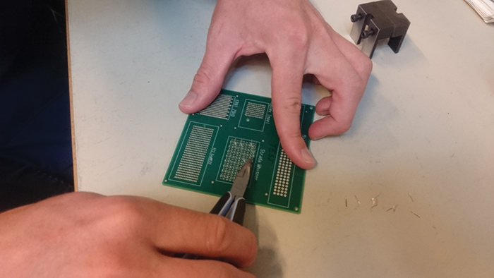
Figure 34. Removal of remaining pins on connector E.
Summary. Rework was performed according to the connector manufacturers’ specifications (except for connector A). The insertions did not pose any problems, while removal was performed in many different ways and was found to be more complicated. The questionable removal process for connector A was performed at the site and company where the connector was manufactured with personnel from this site and in a rather gentle way, although with not perfect results.
Altogether, the rework of these connectors was performed in ways that reflect how the connectors would be reworked on real products.
Tests and Results
After reworking zero, once, twice or three times, test boards were either sent for gas tightness testing, followed by cross-sectioning, or to insertion and retention testing.
For the boards sent to gas tightness test and cross-sectioning, the last inserted connectors remained on the board. The rework flow for these boards is shown in FIGURE 35. For boards designated to undergo single pin insertion and retention force tests, the following rework process flow was used instead. All the boards from the extra rework run for connector B (because of too much board warpage during the main rework test) are shown in FIGURE 37.
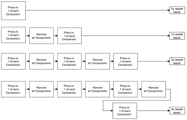
Figure 35. Rework flow chart for connectors on boards intended for gas tightness test and cross-sectioning.
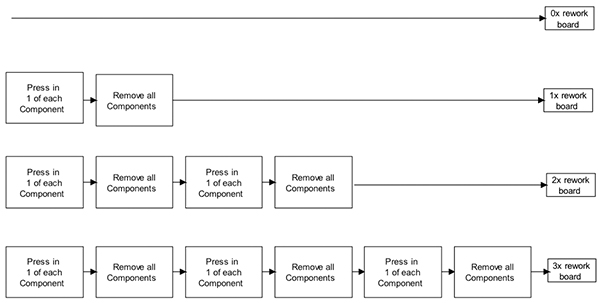
Figure 36. Rework flow chart for connectors on boards intended for insertion and retention force tests.
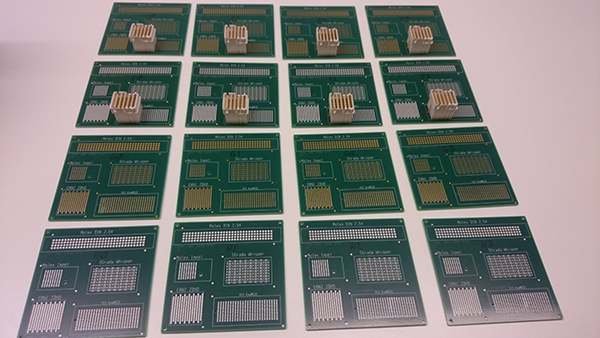
Figure 37. Boards where connector B had been reworked 0 to 3 times ready to be sent to gas tightness test followed by cross-sectioning (boards with connector B) and to insertion and retention test (boards with no connector).
Boards with no connector (marked G0, G1, G2, G3 and H0, H1, H2, H3) were made for insertion and retention tests, while boards with connector B (marked E0, E1, E2, E3 and F0, F1, F2, F3) were made for gas tightness tests and cross-sectioning.
The different tests and measurements performed after the rework and their results are described below.
Single pin insertion and retention force measurements. To evaluate how the strengths of the press-fit connections are affected by multiple reworks for the tested connectors, single pin insertion forces and retention forces have been measured.1 The insertion and retention tests followed the standard Telcordia GR-1217-CORE.1
Single pins were vertically inserted and then pulled out from the plated holes in the test boards. The maximum insertion and extraction forces were then noted for each combination of pin, hole size and hole plating. An example of a force versus displacement plot from the insertion and retention test is shown in FIGURE 38 (online). The maximum force in Figure 38 is the insertion force, and what appears as the minimum force is the extraction force. Both forces were recorded for analysis.
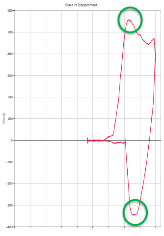
Figure 38. Force versus displacement plot.
Tests and process. The insertion and retention test was performed with single pins from each connector. A total of 240 pins of each pin type were used in this test, which gives 40 pins for insertion and retention for each combination of hole plating (ImSn and ENIG) and hole size (min., nom., max.).
A pull/shear tester with the ability to push or pull 490N was used in the insertion and retention test.
During the insertion and retention test, the pins were first aligned to the center of the holes and then inserted 1.4mm at the insertion speed of 100mm/s. The hold time between insertion and retention was 3s. Then the pins were pulled out at a speed of 100mm/s. All measured insertion and retention forces were saved for analysis. Insertion and retention of the single pins were performed according to the specification without any problems.
A performed design of experiment (DoE) included five different factors with two and up to five levels each (TABLE 7).
Table 7. Factors and Levels for Insertion and Retention Tests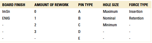
Insertion Test Results. For the insertion force, the model created from the DoE explains the data very well (R-sq = 96.4%). Interaction plots for the insertion force for the connectors A, B, C and E are in FIGURE 39. The data from the reference connector D are much bigger and will be discussed separately (see A.7). In FIGURES 40 to 42, the connectors A, B, C, D and E are referred to as vendor 1, vendor 2, vendor 3, vendor 4 and vendor 5.
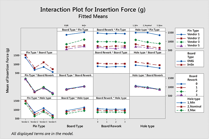
Figure 39. Interaction plot for insertion force – fitted means (vendor 1 = A, vendor 2 = B, vendor 3 = C and vendor 5 = E).
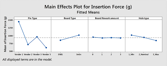
Figure 40. Main effect plot for insertion force - fitted means (vendor 1 = A, vendor 2 = B, vendor 3 = C and vendor 5 = E).

Figure 41. Interaction plot for retention force – fitted means (vendor 1 = A, vendor 2 = B, vendor 3 = C and vendor 5 = E).
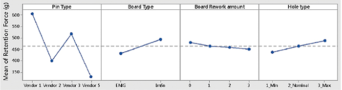
Figure 42. Main effect plot for retention force – fitted means (vendor 1 = A, vendor 2 = B, vendor 3 = C and vendor 5 = E).
As can be seen in the interaction plot for the insertion force, connector A has the highest insertion force, followed by connector C, connector B and connector E. The insertion force is higher for ImSn compared to ENIG for all four connectors, and the insertion force is higher for the smallest holes, lower for nominal holes and lowest for the biggest hole sizes. None of these results is surprising when taking into account the different pin sizes and geometries, as well as that the PCB hole diameters are slightly bigger for the ENIG holes compared to the ImSn holes.
The most interesting results in the insertion test were that there was no significant difference in insertion force when pressing in pins into holes where 0, 1, 2 or 3 reworks previously had been performed. This indicates the hole damage during rework is small.
The main effects from the insertion test are plotted in Figure 42.
A full nested ANOVA analysis from the insertion force tests shows about 84% of the variance in insertion force are due to pin type (from connector A, B, C or E), 9% are from board type (ImSn or ENIG), 4% are due to hole type (min., nom., max.), 3% are due to error and 0% (!) are due to amount of board rework (0, 1, 2 or 3 times).
Retention Test Results. The analysis for insertion test was also performed for retention test data, and the interaction plot for the retention test of connectors A, B, C and E is given below.
Retention force measurements show the same relationship between pin type and hole plating as for the insertion force measurements. (Pins from connector A need highest force to be pulled out, followed by pin C, pin B and pin E. ImSn holes require higher retention force than ENIG holes do). The amount of rework does not affect the retention force much.
The difference between the insertion and retention test is, first, the forces to pull out the pins are much lower than the forces needed to press them in. Another interesting result from the retention test is how the hole sizes affect the retention force. At least for connectors A, C and E, the retention force is higher for the bigger holes than for the smaller ones. This indicates there could be permanent pin deformation during the pin insertion in the smallest holes that make the connection weaker. The main effects from the retention test are plotted in Figure 45 .
A full nested ANOVA analysis from the retention force tests shows about 60% of the variance in retention force are due to pin type (connector A, B or C), 21% are due to error (!), 7% are due to hole type (min., nom., max.), 7% are due to board type (ImSn or ENIG) and 5% are due to board rework amount (0, 1, 2 or 3 times).
For the retention force DoE, much of the data are not explained by the calculated model (R-sq = 77.8%). It was found to be more difficult to estimate and explain the retention force than the insertion force. This implies different types of damages on pins (or holes) are present that are difficult to predict and model.
Reference connector results. As mentioned, the reference connector D has much higher insertion and retention forces compared to the high-speed connectors (A, B, C and E). Reference connector D is also more consequent regarding the insertion and retention forces than the new high-speed connectors are. For the connector D pins, it was always a higher force was required for ImSn compared to ENIG (bigger holes for ENIG); there was no effect from board rework (!) and always higher forces required for small holes compared to the forces for nominal and maximum hole sizes. A sample graph with all five connectors and all insertion force measurement data is shown in FIGURE 43. Figure 43 shows how the inclusion of data from the reference connector D makes it difficult to display differences between the new high-speed connectors (A, B, C and E).
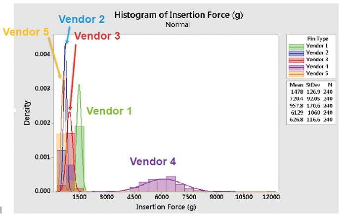
Figure 43. Histogram of insertion force – (vendor 1 = A, vendor 2 = B, vendor 3 = C, vendor 4 = D and vendor 5 = E).
Tests summary. A summary of the insertion and retention tests follows:
- The retention force is always lower than the insertion force.
- All four tested factors (pin type, hole plating, amount of rework and hole size) are correlated to the variance of force.
- Pins from reference connector D have both the highest insertion and retention forces, followed by A, C, B and E. The pins for the reference connector D are much bigger, and forces are stronger in all directions (insertion and extraction) compared to the other tested connectors, so it is not surprising the connections are stronger for the connector D pins. For the evaluated new high-speed press-fit connector pins, the base material thickness and the shape of the needle eye seem to be most important for the connection strength. However, this does not explain all the differences; all geometry and material differences play some role in forming the pin-to-hole connection and affect the strength.
- The insertion and retention forces are higher on ImSn plated holes than on ENIG plated holes.
- The fact that the retention force for max. hole sizes is bigger than for min. hole sizes for connectors A, C and E indicates these pins have permanent deformations, since insertion in the smallest holes weakens the connections.
- The amount of rework has nearly no effect on the pin insertion and retention forces.
The last conclusion is the most interesting in this rework test. Rework of these press-fit connectors does not seem to affect the connection force significantly.
The full report from the insertion and retention tests is indicated in the References.2
Gas Tightness Tests. To investigate if rework of the high-speed press-fit connectors caused cracks or other damages in the hole plating, gas tightness
tests were performed. Tests were performed in accordance with EIA 364, Test Procedure 23.3
Test and process. In the gas tightness test, the electrical interface resistance between the compliant pins and their hole walls was measured for selected pin connections before and after storage in an environment saturated with aggressive gases. The difference in electrical contact resistance indicates the stability of the interfaces.
It was decided to measure the electrical resistance on 13 to 14 pin connections for each combination of component, hole plating and hole size. Examples of chosen pin connections that were measured are given in FIGURES 44 and 45.
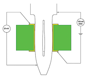
Figure 44. Contact resistance measured in a traditional way by connecting the protruded pin.
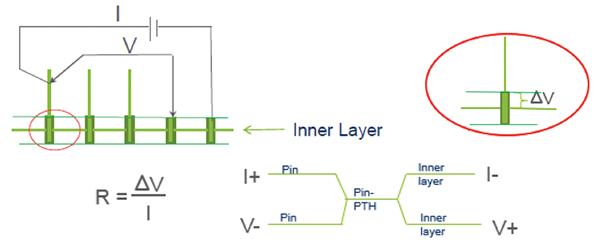
Figure 45. Contact resistance measured by using an innerlayer (when no protruded pins are available).
The interface resistance between pin and hole wall is normally measured by creating an electrical bias between the tip of the pin that protrudes on the secondary side of the board and the top side of the hole plating, and then measuring the current in a circuit between the top side of the pin and the bottom side of the plated holes (FIGURE 46).
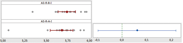
Figure 46. Data distribution (left), 95% C.I. for difference (right) – connector A, 3 reworks, ImSn, min hole.
On the tested press-fit assemblies, only connector D had pins that protruded on the secondary side. The resistance measurement described above could therefore not be used for the new high-speed connectors whose pins did not protrude. Instead, an innerlayer was used to create the electrical circuit. A drawing of this measurement design is in FIGURE 47.

Figure 47. Resistance data in worksheet order, before aggressive gas storage (left) and after the storage (right) – connector B, 3 reworks, nominal hole, ImSn.
The innerlayer measurement method means the resistance from the bulk of the pins and the innerlayer resistance are added to the contact surface resistance. The resistance values in these measurements are therefore higher than normal contact resistance values for the high-speed press-fit connectors.
After the first measurements of the contact resistance between pins and plated hole walls, the boards were placed in test chambers that then were saturated with gases from nitric acid.
After one hour of aggressive gas exposure, the boards were removed from the test chamber, and after another hour of drying, the interface resistances were re-measured. The results from the electrical resistance measurements, before and after aggressive gas storage, were then compared for each measured connection.
Test results. A total of 13 or 14 compliant pin connections were measured for each combination of connector, hole plating, amount of rework and hole size. Even though this is not many measurement points for each combination, altogether about 3,200 measurements had to be performed. Because the hole sizes and many of the pin geometries are close to each other (except for reference component D), the measurements provide good information about how rework affects interface resistance for new high-speed press-fit connectors.
An example of resistance values before and after storage in aggressive gases for assemblies with previously zero, once, twice or three times rework for connector C on ImSn boards for the smallest hole is in TABLE 8. The resistance values do not change much (or sometimes not at all) after storage in aggressive gases after zero to three times rework for connector C. This is true for all the tested combinations of components, plating, hole sizes and amount of rework.
Table 8. Compliant Pin Interface Resistance [mΩ] - Connector C in ImSn Plated, Minimum Size Hholes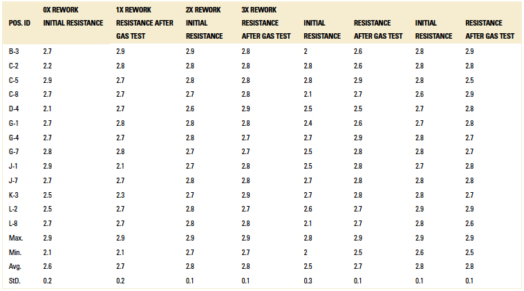
To determine if there could be significant differences between the average measured electrical contact resistance before and after the storage in aggressive gases, 2-sample t-tests were performed for the normal distributions created for each combination of plating, hole diameter, connector and amount of rework. This was performed even though the sample sizes for each single normal distribution are too small to draw statistical conclusions. However, by doing these calculations for all test combinations, general trends and patterns could be estimated. A typical example of the results from these hypothesis tests is in FIGURE 48. The example shows the difference in mean between A3-R-B-I (connector A, 3 reworks, smallest hole, before aggressive gas storage, ImSn plating) and A3-R-A-I (connector A, 3 reworks, smallest hole, after aggressive gas storage, ImSn plating) is 0.061mΩ and that the 95% confidence interval is -0.097 to 0.218mΩ. In other words, there is not enough evidence to conclude the means differ at the 0.05 level of significance.

Figure 48. Data distribution (left), 95% C.I. for difference (right) – connector A, 3 reworks, ImSn, min. hole.
After 2-sample t-tests had been performed for the contact resistance distributions for all 120 combinations of hole sizes, connectors, amount of rework and hole plating, the following could be found:
- No conclusion about significant contact degradation during storage in aggressive gases could be drawn for connector A.
- Connector B had three of 24 comparisons where the contact resistance after aggressive gas storage was higher than before the aggressive gas storage, but it was no logical order regarding hole sizes (1 min., 1 nom., 1 max.) and amount of rework (zero and two reworks, but none with three reworks), and the differences were very small. No conclusion on significant contact degradation could therefore be drawn.
- For connector C, no difference in contact resistance could be found for any combination of hole plating, hole size and amount of rework, except for after three reworks on ENIG where it was consistently higher resistances after aggressive gas storage for all three hole sizes.
- These press-fit connections need to be specially analyzed after cross-sectioning to find out if there are real damages or if the random variation of the measurement data is the only reason.
- As mentioned, there were only 13 measurements for each combination of hole size, hole plating and amount of rework, which is a small sample size to create normal distributions.
- No significant contact degradation during storage in aggressive gases for connector D.
- No significant contact degradation during storage in aggressive gases for connector E.
A comparison between each test combination’s standard deviations was also performed, and no conclusion about consequent differences in the standard deviation of data could be drawn from this hypothesis test (2-sample standard deviation test).
A series of resistance data from before and after aggressive gas storage for connector B, after three reworks, on nominal holes are in FIGURE 49.
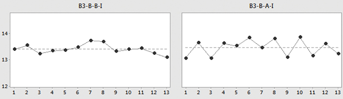
Figure 49. Resistance data in worksheet order, before aggressive gas storage (left) and after the storage (right) – connector B, 3 reworks, nominal hole, ImSn.
Gas Tightness Test. There were very small differences in electrical contact resistance for the different combinations of connectors, amount of rework, hole sizes and plating. The assemblies are stable. Multiple rework had led to no, or very little, hole damage. The full report from the gas tightness test, with all measured contact resistance values, is indicated in the References.
Cross-sectioning. Horizontal and vertical cross-sections were performed following Telcordia GR-1217-CORE and judged by IPC/J-STD-001F,5 IEC 60352-5M Ed. 3/CD6 and IPC-6012B.7 Each component was cut from the board (together with the inserted pins and the board) and then cut in two parts: one for vertical cross-sectioning, the other for horizontal. After being divided in two, each part was mounted in epoxy, and then milling and polishing was performed. Only boards subjected to zero rework and three reworks were cross-sectioned.
Vertical cross-sectioning. Vertical cross-sectioning was performed in automatic milling and polishing equipment that made it possible to receive good centered views of whole rows of inserted connector pins (FIGURE 50). Another cross-section that shows a whole row of signal pins for the connector A is in FIGURE 51.
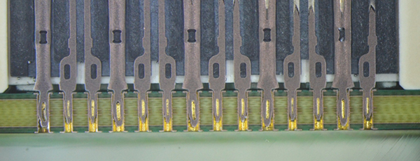
Figure 50. Vertical cross sectioning of connector B.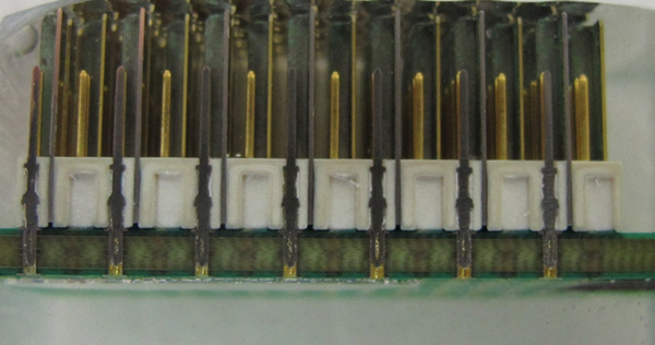
Figure 51. Vertical cross sectioning of connector A.
The cross-sections do not show much hole deformations or hole damage for any of the tested connectors, amount of previous preformed rework or type of hole plating. However, pin deformation increased when pressing into the minimum specified hole diameters, and this resulted, in many cases, in permanently deformed needle eye pins. The limit for elastic deformation was passed, and plastic deformation took place. FIGURES 52 to 55 show examples of this for signal pins for connectors A, B, C and E.
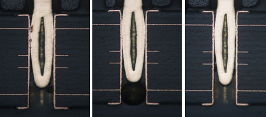
Figure 52. Vertical cross-sectioning of connector A, ENIG plating – maximum specified hole diameter (left), nominal diameter (middle) and minimum diameter (right).
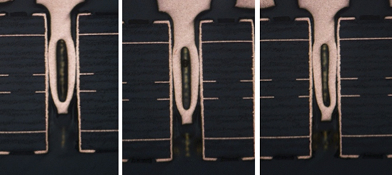
Figure 53. Vertical cross-sectioning of connector B, ENIG plating – maximum specified hole diameter (left), nominal diameter (middle) and minimum diameter (right).
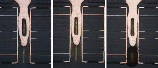
Figure 54. Vertical cross-sectioning of connector C, ENIG plating – maximum specified hole diameter (left), nominal diameter (middle) and minimum diameter (right).
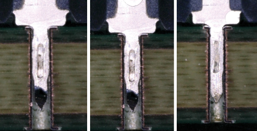
Figure 55. Vertical cross-sectioning of connector E, ImSn plating – maximum specified hole diameter (left), nominal diameter (middle) and minimum diameter (right).
A closer look at the contact surfaces shows only a few and small damaged sites, but also that the actual contact surface area often was rather small. Examples of this are in FIGURE 56.
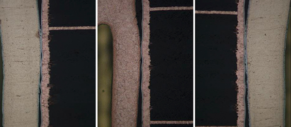
Figure 56. Close view of contact surfaces – connector A (left), B (middle) and C (right) all in ENIG holes.
The connection type for the reference component D was very different compared to the small new high-speed connector connections. The load was evenly distributed over the hole wall, and there was nearly no hole damage for this big, strong compliant pin.
FIGURE 57 shows photos from a cross-section of reference pin D in an ENIG hole that was previously subjected to three reworks.
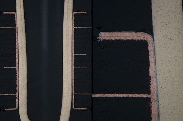
Figure 57. Vertical cross-sectioning of reference connector D, ENIG plating.
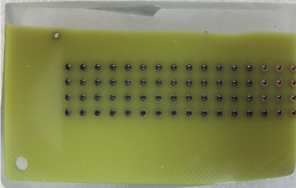
Figure 58. Horizontal cross-sectioning of reference connector D, ImSn plating.
Vertical cross-sectioning did show very limited hole damage for all cross-sectioned components. No lifted pads, cracked hole walls or cracked innerlayers were found. However, in the smallest holes, the high-speed press-fit connector pins were found to have permanent deformations, which is the reason they lost some of their connection strength.
Horizontal cross-sectioning. Horizontal cross-sectioning was performed in such a way that it was possible to have good views of the whole board area of the inserted pins for each component (FIGURE 58, online). Polishing stopped 0.2 to 0.3mm below the top surface of the board. This is a distance that is within the specification of Telcordia GR-1217-CORE, which is 0.3 +0.2/-0.1mm. At this distance from the board top surface, for the new high-speed press-fit connectors, the horizontal cross-sectioning will most often not show the compliant pins in contact with the hole wall. The limits for hole wall deformation are in FIGURE 59. and in the comments below.
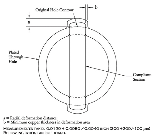
Figure 59. Description of hole deformation after horizontal cross-sectioning, Telcordia GR-1217-CORE.
Dimension “a” in Figure 59 is not allowed to be bigger than 50µm, and dimension “b” has to be measured and recorded according to Telcordia GR-1217-CORE, but no limit is specified.
FIGURE 60 shows two examples from the horizontal cross-sectioning, which is from connector B on ImSn and connector E on ENIG-plated hole. Both photos show pins inserted in minimum hole sizes after three times rework. A photo from horizontal cross-sectioning of a pin connection from the reference connector D is in FIGURE 61.
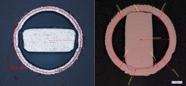
Figure 60. Horizontal cross-sectioning, connector B, ImSn plated hole, 3 times rework (left) - connector E, ENIG plated minimum hole, 3 times rework (right) by connecting the protruded pin.
Figure 61. Horizontal cross-sectioning of reference connector D, ImSn plated hole, three times rework.
The horizontal cross-sectioning did not show any hole damage that surpassed the specified limits in Telcordia GR-1217-CORE.
Connector C pins in ENIG holes that had previously been reworked three times underwent special study because of a possible statistical increase in electrical resistance in the gas tightness test, but no hole damage was found on these assemblies. The statistical study of the data from the gas tightness test for these assemblies must have given a false alarm because of the relatively low number of measured pin-to-hole resistances for each combination of pin type, number of reworks, hole plating and hole sizes.
Conclusions and Recommendations
Multiple reworking of a new family of high-speed press-fit connectors was found to have little or no effect on hole damage and connection strength. All tested press-fit connectors could be reworked up to three times if recommended rework processes and tooling are used for each of the tested connectors.
What really does affect the connection strength are the size, material and geometries of the press-fit pins, the hole sizes and the plating of the holes. Of the tested connectors, the reference connector D has the highest connection strength, followed by the high-speed connectors A, C, B and E.
The insertion and retention forces were shown to be higher on ImSn-plated holes than on ENIG-plated holes. Smaller hole sizes for the ImSn-plated holes compared to the ENIG-plated holes in this test could be the reason for this difference.
The connection strength for pins in maximum specified final hole diameters is bigger than for minimum hole sizes for the connectors A, C and E because these connector pins are so much deformed during insertion that permanent plastic deformation takes place. When the pins lose their elasticity, the pressure toward the inner hole walls decreases, and the connection strength becomes lower. The high-speed press-fit connector B does not show any difference at all in connection strength dependent on hole size. This means some plastic pin deformation takes place in the smallest holes. The connection strength should otherwise be higher for the smallest holes compared to the nominal and maximum hole sizes. The plastic pin deformation for connector B is, however, slightly lower than for the connectors A, C and E.
Even though the press-fit pin connections in the minimum diameter holes are gas tight, and there are no big differences in connection strengths compared to the bigger holes, it is recommended the manufacturers of these new high-speed press-fit connectors review their pin designs and the specified minimum final hole sizes, and the suggestion from this study is to increase these limits.
References
1. Telcordia GR-1217-CORE, December 2008.
2. Dennis Willie et al., “HDPUG Press-fit Technical Report FA # 61744,” 2016.
3. EIA 364, Test Procedure 23, “Low Level Contact Resistance Test Procedure for Electrical Connectors and Sockets,” June 2006.
4. Thomas Peel, “Gas Tight Testing on Compliant Pins,” HDP User Group, June 29, 2016.
5. IPC / J-STD-001F, “Requirements for Soldered Electrical and Electronic Assemblies,” July 2014.
6. IEC 60352-5M Ed. 3/CD, “Solderless Connections – Part 5,” February 2012.
7. IPC-6012B, “Qualification and Performance Specification for Rigid Printed Boards,” August 2004.
Acknowledgments
The author is grateful to the following colleagues, HDP User Group members and supporters who have contributed to the development of methods, performed measurements and reviewed the paper:
Ceperi: Tao Lu
Contech Research: Tom Peel
Ciena: David Wice
Dell: Wallace Ables, Jacky Zhang
Ericsson AB: Anne-Kathrine Knoph, Marie Press, Benny Gustafson, Esmail Dastbaravardeh, Ove Isaksson, Torgny Dahl, Jesper Wittborn, Kjell Asp, Roland Westergren, Rolf Alexandersson, Binas Nisic
Erni: Bernd Eifer
FCI: Jeffrey Toran, John Thompson, Jim Kopec
Flex: Francoise Sarrazin, Dennis Willie, Kelvin Wong, Christopher Vu, Jie Lian, Christian Biederman, Wesley Tran
Fujitsu: Jordan Chaney
HDP User Group: John (Jack) Fisher
Molex: Zach Bradford
Nokia: Joe Smetana
Oracle: Karl Sauter
Sanmina: Doug Thomas
Tyco Electronics: Rickard Barrefelt, Per Nordström, Magnus Andersson, Doug Lawrence, Victor Torres
All component lead photos and the component lead measurements in this report were taken by Jesper Wittborn or Torgny Dahl at Ericsson (Kista, Sweden). The insertion and retention tests in this study were performed by Dennis Willie, Francoise Sarrazin, Kelvin Wong, Jie Lian, Christian Biederman, Wesley Tran and Christopher Vu at Flex (Milpitas, CA). All data and images from the insertion and retention tests were created by them. The gas tightness test was performed by Tom Peel and his staff at Contech Research. All data and pictures in this report from the gas tightness test are from Contech Research. The cross-sections were performed by CEPERI or Tyco Electronics.
Ed.: This article was originally published at IPC Apex Expo in February 2017 and is reprinted here with permission of the author. The evaluation was performed in the High Density Packaging User Group.
is a product engineer at Ericsson AB (ericsson.com); lars.bruno@ericsson.com.


Press Releases
- XLR8 EMS Welcomes Raul Jorge Lopez Jr. as Director of Program Management and Procurement
- Koh Young America Promotes Ramiro Mora to Lead Service and Applications in Mexico and South America
- ViTrox Americas Welcomes Huy Pham as Technical Support Engineer
- XLR8 EMS Appoints Steve Dutton as Chief Sales Officer