

The Future of Through-Hole Technology
Will through-hole components become obsolete?
With the development of surface mount technology (SMT), it was predicted that through-hole components would be phased out and disappear. Will through-hole components become obsolete? Although use of through-hole components has decreased significantly since SMT was developed, through-hole technology will stay in place for years to come. Here we look at the advantages of through-hole components, challenges of through-hole soldering, mitigation methods to these issues, and the revolution and future of through-hole technology.
Through-hole technology is a process by which a plated through-hole (PTH) component is soldered into drilled holes on a printed circuit board (PCB). Through-hole technology was dominant for years in electronics assembly until surface mount technology became available in the 1980s. Today, the majority of components in a product are surface-mount packages. About 5% of components in commercial products are PTH components, and about 10 to 15% of components used for aerospace applications are through-hole. Although use of PTH components is low compared to SMT components, most PCBs are still designed with mixed technology (PTH and SMT components). Common PTH components include connectors, DC-DC components, power supply modules, aluminum capacitors, etc. It is predicted PTH technology will continue to coexist with SMT for years to come.
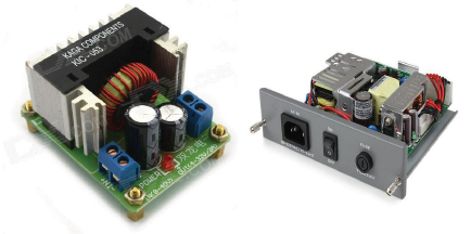
Figure 1. Images of a DC-DC module (left) and power supply module (right). Many PTH components are used in such devices.
PTH advantages. The major advantage of through-hole soldering is its reliability. Unlike SMT, in which the component is soldered on the surface of a PCB, through-hole leads are soldered through the board. This provides stronger connections between layers and permits the part to withstand more environmental and mechanical stress. For example, a through-hole connector is much more reliable than a surface mount connector, and is less likely to fall off during insertion and detachment operations. Our previous studies1,2 on PTH reliability show a PTH solder joint can last for a very long time. No solder failure is expected before 10,000 thermal cycles if the pin wet length of the PTH joint is at least 30 mils1 (TABLE 1).
Table 1. Solder Failure-Free Life of PTH Solder Joints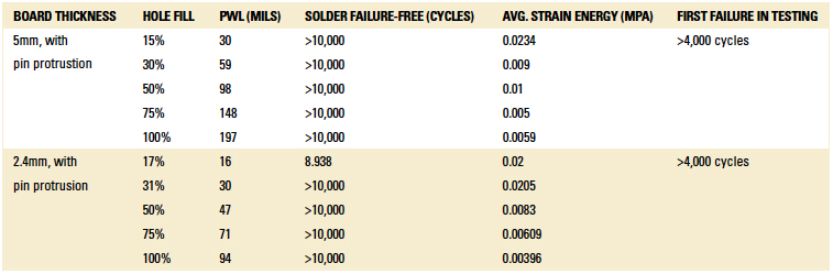
Through-hole components are common in power supply or DC-DC modules. These devices generate a lot of heat and can consume a lot of power. Since through-hole components can dissipate more power than SMT parts, it’s much easier and cheaper to use PTH in these applications than to design a board with very thick copper to dissipate the same amount of power. In addition, when dealing with high voltage, flashover or board creepage, distance is critical, and use of through-hole components is more favorable in the design. Besides, not all components are available as surface mount packages. Sometimes through-hole components are the only option. In many cases, PTH components are cheaper than SMT components for certain applications. Today, through-hole components are still used in high-reliability products such as infrastructure, automotive, military and aerospace products, and in many consumer products. FIGURE 2 shows an example of a computer motherboard. Although SMT components are dominant, many PTH components are still used.
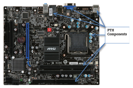
Figure 2. Example of a computer motherboard. Many PTH components are used.
Challenges of PTH soldering. Despite reliability advantages, through-hole components have many challenges. First, through-hole takes up more board real estate than SMT. Second, through-hole increases fabrication costs because it is more expensive to drill holes into the board than form pads on the PCB surface. Third, through-hole component placement and soldering process are time-consuming compared to SMT assembly. Finally, through-hole soldering faces many challenges with Pb-free alloys.
One common issue with through-hole soldering is hole fill. With Pb-free soldering, it is more difficult to achieve good hole fill for PTH components, especially at the through-hole locations that connect to heavy copper ground planes or when a thick PCB is used. Pb-free solder doesn’t spread and wet as well as SnPb solder.
Therefore, it is more difficult for the solder to flow up the barrel. Besides, the process window for Pb-free wave soldering is narrower than SnPb wave soldering and makes it more challenging for hole fill. SnPb solder melts at ~183°C, and the typical SnPb solder pot temperature is ~245° to 255°C. This makes the difference between the pot temperature and melting temperature around 62° to 72°C.
Among the Pb-free solder alloys, SAC 305 melts at ~217°C and SnCu or SnCuNi at ~227°C. The typical Pb-free wave solder pot temperature is around 260° to 270°C. The difference between the Pb-free solder pot and the solder melting temperature is ~43°C. The smaller the gap between the solder pot temperature and solder melting temperature, the less solder capillary action occurs, which can result in less hole fill. Further, when the barrel connects to internal ground planes, the copper ground planes act as heat sinks that take away heat from the barrel and prevent solder from flowing up the barrel sufficiently. It is observed that hole fill issues frequently happen to some PTH components such as aluminum capacitors, RJ-45 connectors and DC-DC or power components. These components’ bodies absorb a lot of heat during wave soldering, which makes it difficult to fill the barrel (FIGURE 3).
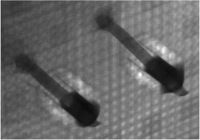
Figure 3. X-ray of aluminum capacitor with poor hole-fill.
The other major challenge of through-hole soldering is copper dissolution. Copper dissolution is a natural metallurgical reaction in which copper dissolves in a Sn-rich liquid. Copper dissolution is not a new phenomenon. It occurs during the SnPb soldering process. However, copper dissolution becomes more noticeable during Pb-free PTH soldering due to the high tin content of Pb-free alloys. Common Pb-free wave alloys such as SAC 305 (96.5Sn3.0Ag0.5Cu), SnCu or SnCuNi alloy contain 96 to 99% of tin. Copper dissolution can occur during wave or selective soldering, and is typically seen during PTH rework where the solder contact time requirement is long. Copper dissolution may impact product reliability. Thinning or missing of copper plating thickness at the knee location can reduce solder joint reliability.3 A cross-section of copper dissolution is shown in (FIGURE 4).
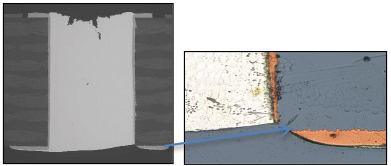
Figure 4. Copper dissolution examples.
Hole fill optimization and copper dissolution mitigation. Hole fill can be improved by process parameters and design. There are many published studies2,4 on process optimization for Pb-free wave soldering. Here is a process-solving strategy for the hole-fill issue.
First, it is essential the through-hole component have lead protrusion during wave soldering. Pin protrusion helps maintain the heat of the pin during wave soldering, and helps solder flow up the barrel more easily. Second, select the correct wave flux material for hole fill. Proper selection of wave flux material can improve hole fill 25% to 30%. A good wave flux typically survives a higher process temperature than required for Pb-free processes. When selecting a Pb-free wave flux material, it is recommended the material should survive preheat temperatures of at least 120° to 140°C. Third, optimize the process for each product. The key process parameters for hole fill are solder contact time, solder pot temperature, preheat temperature and wave environment. Longer contact time and higher solder pot and preheat temperatures should be used when there is a hole-fill issue. Also, use of nitrogen in PTH wave soldering improves hole fill and reduces dross formation.
Higher solder pot temperature and longer contact time result in better hole-fill, but higher pot temperature and longer contact time can result in copper dissolution. The previous studies5,6 show contact time and solder temperature are the most significant process factors that impact copper dissolution. To prevent copper dissolution during PTH soldering, a contact time of less than 10 to 12s and a pot temperature of <270°C should be used for SAC 305. When a PTH component needs to be reworked, a two-step rework process is recommended to minimize copper dissolution. Some Pb-free alloys such as SnCuNi help to slow copper dissolution and are used in PTH rework or wave soldering. However, hole fill and copper dissolution go hand-in-hand and have related effects. Process factors that help with hole fill may cause more copper dissolution. Additive elements such as Ni, Cu, Ge, Sb, etc. added to the solder alloy will inhibit dissolution, yet may also inhibit wetting of the solder to the PTH. Pb-free PTH soldering should be optimized for each product to maximize hole fill and minimize copper dissolution.
There are many challenges in through-hole soldering, but use of PTH components is unavoidable in many products. Pin-in-paste reflow techniques have increased for through-hole soldering. In this approach, solder paste is printed on the through-hole pad, and the through-hole devices are reflow-soldered at the same time as the SMT components. If the solder volume is insufficient to fill the barrel, solder preform can be added and placed in the solder paste to increase solder volume.
Paste in through-hole technology can only be used when the PTH component can withstand the reflow temperature associated with the Pb-free solder paste.
Another trend is to use low-temperature solder paste, SnBiAg for instance, to solder all the through-hole components instead of wave soldering. Wave soldering is considered a second operation and additional process step requiring more labor and time. If through-hole components are soldered at the same time as surface mount components, significant savings in assembly costs, including material and energy, will be achieved.
References
1. Dongji Xie, Ph.D., Billy Hu, Jennifer Nguyen, Dongkai Shangguan, Ph.D. and David Geiger, “FEA Study of Solder Hole Fill Impact on the Reliability of PTH Solder Joints,” IPC Apex Proceedings, March 2009.
2. Jennifer Nguyen, Robert Thalhamer, David Geiger, Dan Rooney, and Dongkai Shangguan, “Reliability Study of Pb-free Wave Soldering for Large Thick Boards,” SMTA International Proceedings, October 2007.
3. Craig Hamilton, Polina Snugovsky, Mario Moreno, Teng Hoon Ng, Juthathip Fangkangwanwong, Matthew Kelly and Marie Cole, “Does Copper Dissolution Impact Through-Hole Solder Joint Reliability?” SMTA International Proceedings, October 2009.
4. Jennifer Nguyen, David Geiger, Robert Thalhammer, Harald Fockenberger and Dongkai Shangguan, “Large and Thick Board Pb-free Wave Soldering Optimization,” IPC Apex Expo Proceedings, February 2007.
5. Jennifer Nguyen, David Geiger, Dongkai Shangguan, and Helmut Kroener, “The Effect of Copper Plating Processes and Chemistries on Copper Dissolution,” IPC Apex Expo Proceedings, March 2009.
6. Craig Hamilton, Matthew Kelly and Polina Snugovsky, Ph.D., “A Study of Copper Dissolution During Pb-Free PTH Rework Using a Thermally Massive Test Vehicle,” SMTAI Proceedings, October 2006.
is owner of JNK Engineering and Consulting (jnkengineering.com), a provider of engineering services and consultancy in electronics manufacturing. She has years of experience in new technology development, process development and deployment, material evaluation, and PCBA assembly. She also has expertise in design, failure analysis, and reliability. She has researched and published numerous papers on nanotechnology, water-resistant coatings, P-free alloys, bottom termination components, Pb-free wave soldering, copper dissolution, no-clean flux reliability, and solder joint reliability. She has led and participated in many consortia projects such as iNEMI and HDPUG projects. She holds a master’s in electrical engineering and a bachelor’s in chemistry/biochemistry from San Jose State University; jnkengineeringservices@gmail.com.


Press Releases
- Javad EMS Upgrades Through-Hole Soldering Capacity with New SEHO PowerWave System
- Sharpen Your Selective Soldering Skills with Kurtz Ersa's July VERSAFLOW 4/55 Training
- Omron Advances Inspection Technology with NVIDIA Omniverse and Metropolis
- Seika Machinery’s SMI 2026 Webinar Series Continues with Focus on PCB Cleaning Before Solder Paste Printing