

CyberOptics to Share Technical Presentation About Best-in-Class Airborne Particle Sensing Processes at PhotoMask Japan
Minneapolis, Minnesota — March 31, 2021 — CyberOptics Corporation (NASDAQ: CYBE), a leading global developer and manufacturer of high-precision 3D sensing technology solutions, will present a technical paper at PhotoMask Japan on April 20th at 6 p.m. CDT / April 21st at 8 a.m. JST.
Ms. Vidya Vijay, Senior Program Manager, CyberOptics, will present the technical paper titled ‘Improving Yields and Tool Uptime with the In-Line Particle Sensor in Semiconductor Environments.’
Minimizing particles in semiconductor fab environments remains a critical success factor. Stringent manufacturing requirements and a focus on maximizing yields and tool uptimes drives a need for best-in-class practices for a contamination-free process environment. Quickly identifying when and where airborne particles originate, as well as the source of the contamination, proves challenging.
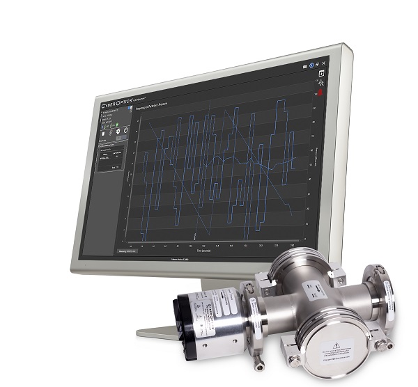
To address this critical need, an In-Line Particle Sensor (IPS) can be used for effective semiconductor tool set-up and process diagnostics. The device and accompanying CyberSpectrum software can identify, measure, monitor and troubleshoot particles down to 0.1µm in gas and vacuum lines 24/7/365 in semiconductor process equipment.
The IPS is an extension of the industry-leading WaferSense and ReticleSense Airborne Particle Sensors (APS and APSRQ) that are documented by fabs as the Best-Known Method (BKM). Combined with CyberSpectrum software, it is particularly relevant for EUVL tools where the ability to monitor particles in-line can significantly improve EUVL tool yield and productivity. For example, it can be installed at the vacuum line in between the EUV process chamber and the vacuum pump, saving significant time compared to current methods of sending a monitor dummy reticle into the EUV system to check for particles before and after sending the reticle into the EUVL. The IPS is always on and collecting particle data, which is especially critical during chamber purging.
Process and equipment engineers can speed up equipment qualification with real-time, 24/7 monitoring, compare past and present data, as well as one tool to another. Contamination sources can be identified quickly and the effects of cleaning, adjustments and repairs can be seen in real-time. Fabs can shorten equipment maintenance cycles, lower equipment expenses and optimize preventative maintenance plans. Overall, by adopting the IPS solution, fabs can recognize significant reductions in time and expense while improving yields and productivity.
For more information, visit www.cyberoptics.com.
About CyberOptics
CyberOptics Corporation (www.cyberoptics.com) is a leading global developer and manufacturer of high-precision 3D sensing technology solutions. CyberOptics’ sensors are used for inspection and metrology in the SMT and semiconductor markets to significantly improve yields and productivity. By leveraging its leading edge technologies, the Company has strategically established itself as a global leader in high precision 3D sensors, allowing CyberOptics to further increase its penetration of key vertical markets. Headquartered in Minneapolis, Minnesota, CyberOptics conducts worldwide operations through its facilities in North America, Asia and Europe.
Statements regarding the Company’s anticipated performance are forward-looking and therefore involve risks and uncertainties, including but not limited to: a possible world-wide recession or depression resulting from the economic consequences of the COVID-19 pandemic; the negative effect on our revenue and operating results of the COVID-19 crisis on our customers and suppliers and the global supply chain; market conditions in the global SMT and semiconductor capital equipment industries; trade relations between the United States and China and other countries; the timing of orders and shipments of our products, particularly our 3D MRS SQ3000 Multi-Function systems and MX systems for memory module inspection; increasing price competition and price pressure on our product sales, particularly our SMT systems; the level of orders from our OEM customers; the availability of parts required to meet customer orders; unanticipated product development challenges; the effect of world events on our sales, the majority of which are from foreign customers; rapid changes in technology in the electronics and semiconductor markets; product introductions and pricing by our competitors; the success of our 3D technology initiatives; the market acceptance of our SQ3000 Multi-Function inspection and measurement systems and products for semiconductor advanced packaging inspection and metrology; costly and time consuming litigation with third parties related to intellectual property infringement; the negative impact on our customers and suppliers due to past and future terrorist threats and attacks and any acts of war; the impact of the MX3000 orders on our consolidated gross margin percentage in any future period; risks related to cancellation or renegotiation of orders we have received; and other factors set forth in the Company’s filings with the Securities and Exchange Commission.
PCB EAST: The original East Coast technical conference and exhibition! Returning to the Boston suburbs in June 2021!


Press Releases
- Altus Adds LPKF CuttingMaster 3290 to Depaneling Portfolio
- Kurtz Ersa Partners with E-tronix for Sales in Illinois and Wisconsin
- XLR8 EMS Welcomes Raul Jorge Lopez Jr. as Director of Program Management and Procurement
- Koh Young America Promotes Ramiro Mora to Lead Service and Applications in Mexico and South America