

2013 Articles
The road less traveled is often the fastest.
Sometimes a circuit board can be populated much quicker than a machine can solder it. If you find that boards are piling up waiting for the machine to finish, there are a number of different ways to reduce the throughput time. I will address one of them this month.
When drawing a path for the machine to follow, begin your next path close to where your previous path stopped. A machine that travels a long distance, crisscrossing back and forth around the board, will dramatically increase cycle time and decrease efficiency.
I know this sounds obvious, but by being diligent with this practice, we have decreased cycle times by as much as 50%. How? When you first program the board, you may not have considered every little detail. Once a couple of boards have been run for the first time, issues begin to appear, such as a missing part or the nozzle making contact with a bottom-side surface mount part. The natural response is to go into the program and add a couple of new paths. But each occurrence adds complexity, and if you’re adding complexity without considering where your machine needs to travel, the result will be a lot of time wasted with the nozzle traveling all around the board.
Chris Denney is chief technology officer at Worthington Assembly (worthingtonassembly.com); cdenney@worthingtonassembly.com.
http://circuitsassembly.com/cms/images/stories/ArticleImages/1305/soldering.jpg
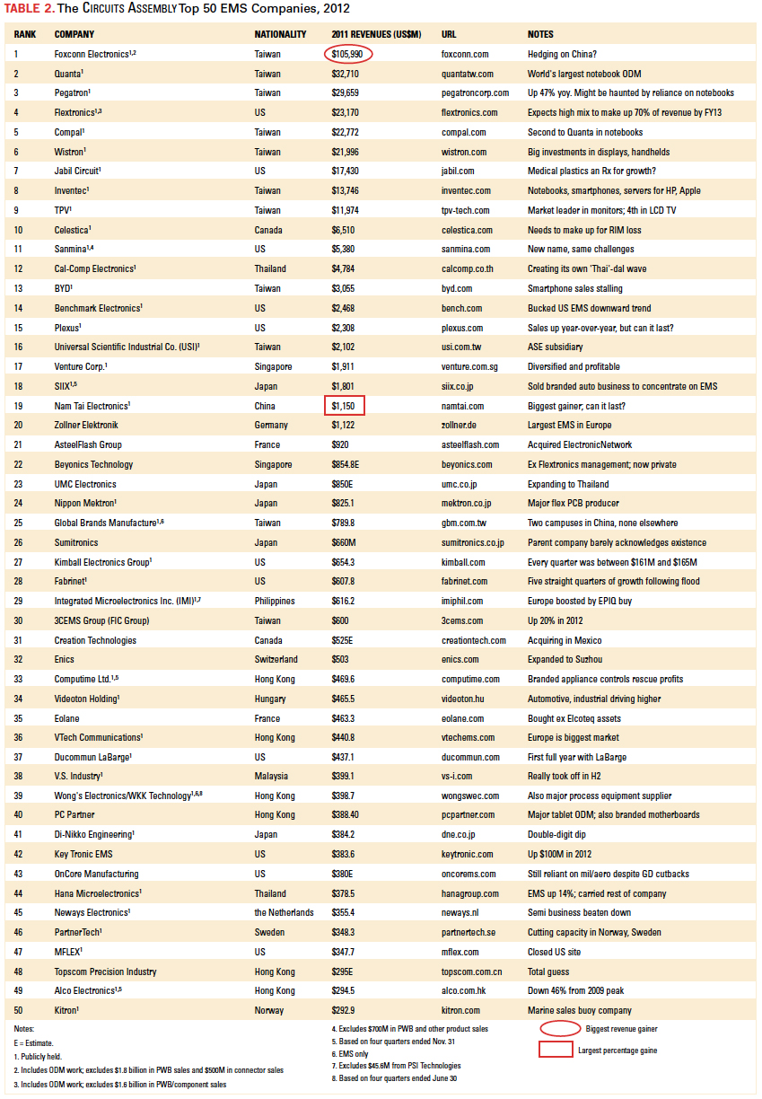
EMS companies showed their flexibility in 2012, adjusting to slowing consumer and defense markets.
2012 was a reminder of the somewhat fragile nature of the customer-manufacturer outsourcing relationship.
A pair of Top Tier EMS companies absorbed potentially staggering blows from the losses of their largest customers in 2012, a year in which a heretofore fast-growing mid-tier EMS also saw its largest customer shrink.
To recap, in June, RIM announced it would cut ties with Celestica. (RIM also dumped Flextronics.) Then in the third quarter, Juniper let it be known it would depart from Plexus. This was an even bigger surprise, as Juniper not only made up 16% of Plexus’ sales, but had been the EMS firm’s largest customer since 2003.
Also, General Dynamics trimmed its relationship with No. 43 OnCore, and No. 29 Fabrinet’s largest customer, Oclara, terminated their relationship, although that move was seen as a negotiating ploy.
Elcoteq, RIP. To see what the loss of a leading customer can do, we need look no further than Elcoteq. With the loss of Nokia, the once-massive Elcoteq business evaporated, although to where, no one seems entirely sure. One likely suspect: Eolane. While as of March last year, the bankrupted Elcoteq had shuttered a total of seven operations in Shenzhen, Switzerland, Finland, Luxembourg and Mexico, Eolane, the French EMS, was busy acquiring its sites in Estonia and India. It’s a sad demise for Elcoteq, which ranked sixth in revenues among EMS companies as recently as 2008.
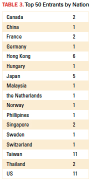
Meanwhile, No. 35 Eolane has emerged as France’s second-largest EMS, behind No. 21 AsteelFlash. (France did not have an entry on our original list, which covered calendar 2008.) Both firms are looking at additional growth through acquisitions, with AsteelFlash having gobbled up former Top 50 entrant ElectronicNetwork in August.
2012 was a tough year for most EMS companies. Outside of M&A activity, it’s tough to grow when the end-markets are sliding.
At least a dozen companies declined year-over-year, with Flextronics leading the way thanks to its changing business model, which saw it exit the low-margin PC ODM business. Celestica and SIIX were among the largest revenue decliners, but SRI Radio Systems arguably had the worst year, declaring insolvency before being snapped up by TQ-Group of Germany.
A record 20 companies topped the $1 billion mark, although that comes with the disclaimer that this year we began including the ODMs (see below). Foxconn grew the most, up nearly $13 billion (slightly more than the size of Celestica and Sanmina combined). The newest entrant, No. 19 Nam Tai, was also the biggest gainer, up a startling 91% (not a typo) from 2011. Mergers and acquisitions notwithstanding, other big winners included No. 25 GBM, No. 30 3CEMS, No. 33 Computime and No. 42 Key Tronic.
The ODM effect. Hardcore Circuits Assembly Top 50 watchers might ask, “Where did all these Taiwanese companies come from?” The answer is they were always around, just not included. The reason: ODMs have for various reasons traditionally been excluded from EMS company lists.
Lately, we’ve found the rationale for separating the two groups weak. ODMs generally compete with EMS companies for business in certain large sectors (computing, networking, consumer), and several so-called EMS companies (Foxconn, Flextronics, 3CEMS, Sanmina, to name a few) have for years operated what analysts refer to as ODM businesses. No list we know of has discounted the ODM sales from EMS revenue, however. Instead, they seem to dismiss most of the Taiwan ODMs, yet include their Western counterparts. By definition, an ODM designs and manufactures a product to be branded by another firm. Every electronics end-product that’s sold is branded in one way or another. And ODMs today are chasing margins as much as markets, meaning they are coming in closer competition with the “pure” EMS firms. We find the distinction between EMS and ODM too fine to be relevant today, thus the presence of several “new” listings.
To muddy the waters further, not every company that is called an ODM meets that definition. Two big Acer spinoffs, Qisda and BenQ, sell primarily their own branded goods. Thus, they aren’t listed here. On the other hand, Wistron, another Acer spinoff, makes the list because the IT, computer and consumer electronics it designs and builds are on behalf of OEM customers, as does TPV, despite a joint venture last spring that left it owning 70% of Philips’ TV division.
Insofar as successes in 2012 went, Nam Tai’s surge was the story of the year. The China-based company finally saw its investments in LCD modules for smartphones and tablets pay off, and was aided by sales of LCDs to the automotive industry, particularly US OEMs.
Can it last? Nam Tai has invested heavily in capacity in southern China, and has another 1.2 million sq. ft. “parcel” of land that it plans to develop – twice the size of its present Shenzhen campus. This is all the more amazing because Nam Tai says its two existing factories are capable of about $150 million in revenue per month each, which suggests its current capacity utilization is around 30%.
Hits and misses. We overstated OnCore’s revenue last year. We pegged it at $640 million on the basis of incorrect information that Victron, which it acquired, had much higher sales than it did. The correct revenue was $420 million, per the company. And the rule of thumb for flex PCB producers is that 40% of their revenue comes from assembly. Unfortunately, we miscalculated for Nippon Mektron last year and inadvertently gave it credit for 60%. Finally, apologies to 3CEMS, which we listed as a Chinese company, when in fact it is Taiwan-based.
All company revenues reported here are converted to US dollars (Table 1), and to the extent possible, we use calendar 2012, regardless of any individual company’s specific fiscal year. Because of differences in fiscal years and constantly fluctuating currency rates, company-reported revenues might vary somewhat from what is shown here. As always, any errors are our own.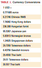
For those who are wondering which EMS companies might have made the cut had we continued the practice of ignoring most of the major ODMs, that partial list would include (alphabetically) CTS, Scanfil, Selcom, SVI Public Co. and TQ-Group.
[Ed.: To enlarge the figure, right-click on it, then click View Image, then left-click on the figure.]
Mike Buetow is editor in chief of PCD&F and Circuits Assembly; mbuetow@upmediagroup.com.
Ed: For the 2011 Top 50, click here.
For the 2010 Top 50, click here.
For the 2009 Top 50, click here.

Reducing solar silver costs using a dual-print process.
More than a year ago I wrote of the use of certain printing strategies to help offset the high cost of silver (“Solar Strategies to Offset the Rising Cost of Silver,” CIRCUITS ASSEMBLY, September 2011). These ranged from the advancing accuracy of screen technology and metallization print platforms (which, by the way, have already helped reduce silver paste volume requirements) to print-on-print and dual-print techniques, to a complete change in materials. At the time, these were proven approaches to silver reduction, but I had no practical figures to share. Now I do.
Recently our company partnered with DuPont Microcircuit Materials, a leading manufacturer of photovoltaic metallization pastes, to analyze potential cost-savings and cell conversion efficiency improvements in the manufacture of c-Si solar cells. The cost savings centered on silver paste consumption reductions, a central focus in the photovoltaic market for some time. With silver prices at $1300/kg at the time of our study, cutting cost was more important than ever. The drive to reducing silver use has already led to more efficient grid architectures, including the design of narrower finger widths, moving from the 80 to 90µm range to widths of 50 to 60µm in production. Printing these finer dimension fingers has been achieved through advances in paste technology, print platform capability and improvements in screen production with ultra-fine meshes. However, paste laydown reductions have resulted in thinner busbar paste volumes, so one must be careful to balance this so that subsequent solder adhesion (during the attachment of tabbing ribbons) is not adversely affected.
The work with DuPont MCM utilized several components to analyze single- and dual-print processes and their relative effectiveness in relation to paste reduction, cell reliability and cell efficiency. These elements included DEK-manufactured ultra-fine mesh screens, both traditional and optimized DuPont MCM silver metallization pastes and DEK electroformed nickel stencils. With the single-print process, standard mesh screens were used to print the cell rear side, and ultra-fine mesh screens were used for the front-side grid in total (fingers and busbars) with a latest-generation front-side paste. Using ultra-fine meshes in single-print mode permitted the desired reduction in paste consumption – as much as 30% in this evaluation – as well as slight increases in electrical efficiency but, as I cautioned, did result in reduced solder adhesion forces. Because a finer mesh was used, the busbar area was printed thinner than the minimum required for good adhesion. So, with a single print scenario and ultra-fine screens, we achieved what I would call a win-win-loss: reduced silver paste consumption (win), slight improvements in electrical efficiency (win), and reduced solder adhesion (loss).
Taking the analysis further, the next phase leveraged dual-print techniques to find out if paste laydown reductions, cell efficiency improvements and good solder adhesion could be achieved. For this evaluation, busbars were printed with an optimized – or floating – busbar paste through a 400 mesh (400 wires per inch) screen. The advanced busbar paste is non-contacting and enables the busbar to do its job (conduct current away from the fine lines) and mechanically adhere to the wafer surface without making electrical contact with the wafer itself. Therefore, with the optimized busbar paste – as opposed to the traditional front-side grid paste – less paste can be used without adversely affecting adhesion. In fact, in our evaluation, the optimized busbar paste actually increased adhesion force beyond the normal standard. Next, specialized dual-print electroformed stencils, 30µm thick with 30µm apertures, were used to print the fine finger widths with a standard front-side paste. Because the stencil design permits a 100% open area in the apertures (as opposed to mesh screens), extremely fine lines can be achieved and, therefore, paste consumption reduced further. So, here we have a win-win-win scenario: a relative increase in cell efficiency of >0.5%, reduced paste consumption of up to 40% and higher reliability modules due to the improvement in solder adhesion forces.
With the dual-print process, the rear side is printed, followed by the screen print of the front-side busbars and then the stencil print of the front-side grid/fingers.
With the extra print step, an additional printer is required. But, a detailed cost of ownership analysis reveals that even with the extra equipment costs, the dual-print processes as outlined above yield significant cost savings. Our calculations show that with the dual-print scenario described here and a consistent cell efficiency of 17.25% (note that this assumes no increases in efficiency, although our work showed a greater than 0.5% relative efficiency gain), a cell manufacturer would save $120,000 per year, even taking into account the cost of the additional printer and stencils.
With all the pressure to reduce manufacturing costs and lower the overall price tag of solar power, the results of this work are a tremendous step forward. This is arguably the best current solution for silver paste consumption reduction – one that also improves efficiency and enhances reliability. And work is already underway to advance stencil technologies for, perhaps, a single print solution with similar results. I’ll keep you posted.
For more information on the study conducted by DEK and DuPont, please contact the author.
Tom Falcon is a senior process development specialist at DEK Solar (dek.com); tfalcon@dek.com. His column runs bimonthly.

Press Releases
- Adam Ryder appointed as Managing Director of Incap UK
- Metal Etch Services Opens New Motor City Facility to Meet Growing Midwest Demand
- Yamaha surface-mount line powers the future of specialized production at Inter-Company in Netherlands
- Matric Group Becomes the First U.S. Manufacturer to Deploy Panasonic NPM-GH Dual Lane SMT Technology