

2005 Articles
Novel Conductive Inks for Smart Label Applications
A new silver material delivers low resistivity, stable physical and electrical properties, and a wide processing window.
Recent material advancements have produced a new family of highly conductive silver inks for smart card and label antennas that achieve significantly better and more stable electrical performance, using lower antenna profiles. Low-temperature dry/cure cycles and thinner traces contribute to faster, more efficient processing and better throughput rates. The performance and processing gains contribute to lower cost of ownership.
Frequencies. High-frequency (13.56 MHz) smart card/label systems have a read distance up to one meter, and are well suited to certain medical device applications, which may need a confined range to avoid interference with other sensitive equipment. HF technology relies on inductive coupling, which requires the lowest possible bulk resistance in the antenna material (both volume and sheet resistivity). It is typically used for passive tags, and can be found in applications such as access cards and item level tracking in libraries.
However, in applications where longer read distances (up to three meters) are desired, ultra HF (850 to 950 MHz) or microwave must be employed. UHF is generally used for active tags with an integrated battery or for passive tags with capacitive, E-field coupling. Common applications include pallet-level supply chain management, inventory control, electronic toll collection and postal tracking. In addition to low resistivity, an essential feature of sucessful UHF antenna material is an extremely smooth surface and sharply defined edge features to facilitate the efficient transfer of electrons.
There is also early activity in the microwave range (2.4 to 5.8 GHz), which delivers much longer read distances of 10 to 15 meters and offers the fastest data transfer of any available frequency. Like UHF, it can be used in active tags with an integrated battery or in passive designs. It is currently in limited use in advanced communications, but future labels and cards that operate in this range will offer advantages for supply-chain management, electronic toll collection and other high-speed applications.
Antenna materials. Copper etching remains the incumbent technology in many HF and UHF smart cards, and some smart label systems. Copper antennas require a subtractive manufacturing process, which generates acid byproducts that must be handled and disposed as hazardous wastes. In addition, the formation of copper oxide over time can create reliability problems in UHF applications, as copper oxide is an insulator and will reduce the conductivity of the antenna’s surface. Aluminum antennas pose similar problems with the formation of aluminum oxide, also an insulator.
Among the material advancements helping engineers achieve performance and processing goals is an emerging generation of silver-filled interconnect materials that deliver dramatically lower resistivity, with extremely stable physical and electrical properties. Conductive silver inks have been used for some time for printing antennas, bridges and circuitry, but a new family of products addresses both performance and processing issues encountered in existing applications.
With resistivity levels previously unattainable in silver ink formulations, these materials contribute to faster data transfer and longer read distances. In fact, specific formulations have demonstrated resistivity levels a full order of magnitude lower than existing silver inks. The lower resistivity permits manufacturers to create antennas with smaller form factors, using less ink. In contrast to copper- or aluminum-etched and traditional silver ink antennas, the additives in these formulations dramatically reduce the formation of silver oxides that increase resistivity. Stable electrical performance is maintained and does not degrade over time.
The new conductive inks also offer such significant productivity gains that manufacturers can take advantage of thinner films and lower dry/cure temperatures, contributing to faster throughput and reduced costs in both HF and UHF applications. Based on innovative organic chemistry, the products are designed around silver-filled organic polymers and a proprietary additive combination. The unique chemistry acts upon the silver to dramatically enhance particle-to-particle contact and create a tighter network in the fully-cured or dried materials, delivering resistivity approaching that of etched copper antennas (Figure 1).
| FIGURE 1: Physical and electrical properties of thermoset and thermoplastic silver inks. (Click here to view image) |
These inks deliver a very high-resolution image using conventional screen-printing techniques, with precise features and excellent definition. Yet the elastomeric nature of the cured materials helps enable applications requiring durable and flexible antennas, such as smart cards carried in wallets or labels placed on curved surfaces or stored/transported in rolls.
Electrical properties. The performance jump in electrical properties is due to the additives package in the new products, which removes the lubricants and fatty acids initially brought in with the silver filler. Product engineers hypothesize that this cleaning action helps promote a level of cold welding, which creates a more continuous metallurgical network in the cured materials. This significantly reduces the formation of silver oxides and leads to a marked improvement in electrical performance. The conclusion is well supported by thermal and electrical conductivity data, and long-term environmental stress testing.
The result is significantly lower and far more stable resistivity, especially under electrical and environmental stresses that tend to degrade the performance of conventional silver-filled materials. Unlike traditional inks, the electrical performance of these materials actually improves during environmental stress testing, as shown by the significantly lower resistivity after heat aging (Figure 2). The testing illustrates a predictable drop in resistivity across the entire family of products, which is then maintained throughout the life of the test, demonstrating stability previously not obtained in silver inks.
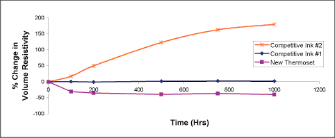 FIGURE 2: Electrical testing of new interconnect materials shows improved resistivity (negative % change) after exposure to thermal stress. |
Processing. The inks can be used on a variety of low-temperature substrates, including PET, PEN, PVC and coated paper. They can be screen- or stencil-printed using standard production equipment. They have also proven effective in high-speed laser ablation, which makes it possible to achieve feature resolutions of 2 to 5 µm. Equally important, ablation eliminates many of the production steps used in copper etching and virtually all of the undesirable effluent.
Screen printing is presently the most efficient and widely used technique, achieving less than 10 µm thicknesses with the capability for high resolution and good throughput to meet current volume demands (Figure 3). The inks are designed to be processed on equipment already in common use.
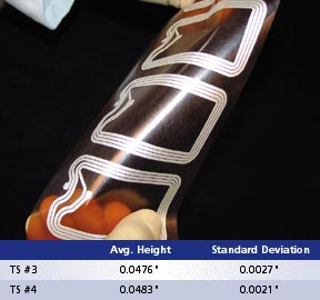 FIGURE 3: Four-turn antenna. (add something re. how screen printed) |
Developing alternative printing methods will be important to achieving high throughput rates in smart label/card applications. Flexographic printing permits a higher throughput than rotary or flat bed screen printing, and also permits a relatively thick printed layer. The technique typically requires low viscosity inks for effective processing.
Much work is focused on gravure and inkjet printing. Gravure would permit very high throughput rates and would also provide some flexibility in pattern design by permitting different amounts of ink to be printed on different areas of an antenna or circuit. Challenges to overcome include the ability to print on rough surfaces and the cost of the printing plates.
Inkjet printing has captured interest, as it can achieve very fine resolutions (to 20 µm) and enables a user to print in more than two axes. Inkjet techniques also provide flexibility in pattern designs and the ability to change designs quickly. The process generates very little ink waste, but requires very low viscosity inks. The material challenge to date has been how to achieve low volume resistivity properties, typically a function of filler loading and type, in a very low-viscosity material.
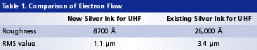
For UHF applications, other critical features of a conductive ink include surface smoothness and high resolution. The new product family includes a formulation designed specifically for UHF applications, with an extremely smooth surface that is achieved by selecting the optimum combination of particle size and filler morphology. Comparisons to existing UHF materials printed using the same screen and antenna pattern indicate superior edge definition and surface smoothness, which facilitates rapid electron flow over the surface of the antenna. By helping the system capture the maximum amount of E-radiation in the field, a smooth surface contributes to the most efficient signal transfer from antenna field to RFID chip and then back out to the antenna field and software.
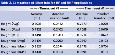
As indicated in Table 1, test data illustrate the difference in surface smoothness between an ink formulated for UHF compared to an ink formulated for HF applications, demonstrating the impact of product selection on smoothness. Matching the proper ink to the specific application can be key for assuring optimal performance. For example, in Table 2, Thermoset #4 (formulated to achieve a very smooth surface) would deliver higher performance in a UHF application than Thermoset #3.
After printing, the materials can be dried (thermoplastics) or cured (thermosets) in standard convection and IR reflow ovens, or on belt furnaces to accommodate high-speed manufacturing operations. Both thermoset and thermoplastic versions offer a range of process options. Inlay manufacturers can specify low-, mid- or high-temperature systems, with a wide spectrum of physical properties and processing options to suit individual manufacturing operations.
The inks form a tenacious chemical bond with the substrate for outstanding adhesion and moisture resistance, while providing a wide process window and reduced cure temperatures. Materials engineers are also evaluating alternative cure mechanisms, including UV and variable frequency microwave (VFM). Aimed at even higher throughput using less energy, the goal is to add setup flexibility and enable new equipment and processes for continuous improvement in manufacturing efficiency. Early work has shown VFM to be a promising cure mechanism for conductive ink antennas, as the technology will heat the ink so rapidly that the substrate does not have time to heat up. This enables the use of higher temperature cure materials on low-temperature, low-cost substrates.
VFM will cure conductive inks in about 1/10 of the time a convection system would take. Depending on the specific thermoset formulation, the new silver inks can be cured in a VFM system in as few as two minutes, or in a thermal system at temperatures as low as 85° (Figure 4).
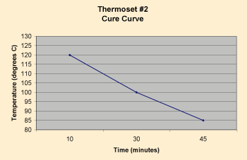 FIGURE 4: New thermoset formulations offer a wide processing window to help match products to specific process conditions. |
New thermoplastic formulations based on this epoxy technology attain such a compact structure after solvent removal (drying) that their conductivity significantly exceeds the performance of conventional thermoplastic silver inks, rivaling the performance of many existing thermoset materials. Although mild heat (85° to 120°C) is recommended to efficiently drive off the solvent carrier, some thermoplastic inks can be dried efficiently at temperatures as low as 40°C (Figure 5). This low-temperature processing ability enables the use of low-cost substrates such as phenolics, polyesters (Mylar and other PETs) and paper. Reduced temperatures, ease of processing and material performance all contribute to a favorable cost structure in the thermoset and thermoplastic versions of these materials.
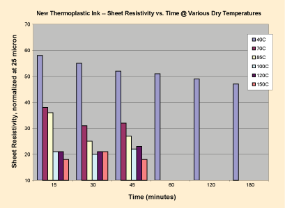 FIGURE 5: New thermoplastic silver inks can be dried at temperatures as low as 40°C. Processing at 70°C or above delivers significantly lower resistivity. |
Future developments. While screen printing is an effective and efficient technique that is widely accepted at present, to meet projected demands for smart labels and cards over the next several years, material suppliers, equipment designers, antenna inlay and tag/card manufacturers will need to collaborate for continued processing advancement. Creating a smart label/card system is a complex interaction, with many contributors whose products and services effect one another. The key parties will need to understand the possibilities and limitations of the others to go beyond flat bed printing techniques.
To achieve the line speeds that can generate label volumes needed to serve the expanding number of applications, flexographic, rotogravure and inkjet printing are the most likely candidates. Materials engineers are already at work developing and testing future generations of interconnect materials, designed to take advantage of true high-volume processing techniques. n
Paul Berry is application engineering center supervisor, Marjorie Dwane is market manager and Greg Butch is senior application technician, Dow Corning Corp. (dowcorning.com); paul.berry@dowcorning.com. Denley Baghurst is applications engineer, Polymeric Interconnect Inc.


Press Releases
- XLR8 EMS Welcomes Raul Jorge Lopez Jr. as Director of Program Management and Procurement
- Koh Young America Promotes Ramiro Mora to Lead Service and Applications in Mexico and South America
- ViTrox Americas Welcomes Huy Pham as Technical Support Engineer
- XLR8 EMS Appoints Steve Dutton as Chief Sales Officer