

2005 Articles
Using Traditional SMT Processes for Semiconductor Packaging
A two-part look at bumping and encapsulation of flip-chip BGAs.
As the lines between semiconductor packaging and PCB assembly move closer, packaging specialists are discovering that traditional SMT equipment and processes can provide cost-effective solutions for package manufacture. In fact, in several applications the disciplines are so close it is difficult to discern where semiconductor packaging stops and PCB assembly begins.
Take, for example, the MCM. This package consists of several individual die placed inside a package, which is then assembled onto a PCB. It is really a miniature system that requires manufacturing processes that encompass both semiconductor packaging and traditional SMT. Many SMT manufacturing processes have been successfully adapted to meet these types of applications.
Indeed, screen printing, historically associated with SMT assembly, provides some unique and cost-effective solutions for semiconductor packaging applications. In my next two columns, I will look at one package type (the flip-chip BGA) and the various manufacturing steps that can be addressed through this technology.
Package basics. The flip-chip BGA incorporates several different packaging processes (Figure 1). As illustrated, production of this package requires five process steps: bumping the chip (or wafer) that will reside inside the package, attaching the chip to the substrate, bumping or ball placement of the substrate for interconnect to the board, underfill and encapsulation of the package. All these processes are effectively addressed via screen printing.
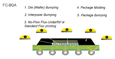 FIGURE 1: Simplified schematic of a flip-chip BGA device.
 |
Wafer bumping and ball placement. While several methods are used to create preformed solder balls on the wafer surface, the main challenge for flip-chip techniques is finding a solution that can deliver high-volume manufacturing cost-effectively. Wafer-level bumping may be used to attach bare die to the substrate and substrate level bumping then provides the interconnect to the board. For larger bump size (0.2-0.9 mm), ball placement is an effective alternative to bumping.
For bumping at the wafer and substrate levels, a simple print and reflow method that permits single stroke, unlimited bump quantity with bump height targets of 80 to 150 µm on pitches of 150 to 500 µm can be used (Figure 2). This technique requires strict application of design rules when creating the stencil, which is generally electroformed. When using this method, it is also critical that the design of the bond pads permits sufficient contact area to achieve good solder joint strength for a given standoff.
 FIGURE 2: Bumped die using print, reflow method. Ball diameter is 80 µm.
 |
Screen printing platforms can be modified to meet these semiconductor packaging requirements with the addition of a wafer handling system; a robust, paperless, cleanroom compatible cleaning system; and a print head capable of delivering controlled paste volume transfer and uniformity. Just as in surface-mount printing, the print head moves across the surface of the stencil, apertures are filled and, through excellent gasketing between the stencil and wafer, the paste volume transfer is uniform. Following reflow and cleaning, the wafer or substrate is ready for the next process step.
Pb-free materials do have an impact on wafer bumping. The rheologies of Pb-free solder pastes are different than SnPb pastes and, just as screen printing parameters must be altered to address the transition in surface-mount assembly, so must they be altered for semiconductor packaging applications. Higher paste viscosity and increased metal content, the non-self-aligning characteristic of the materials and lower wetting forces will require careful attention to stencil material and design, paste deposition method and equipment accuracy for wafer bumping – just as with PCB assembly.
Clive Ashmore is global applied process engineering manager at DEK (dek.com). His column appears semimonthly.


Press Releases
- Zollner Puts a New Mechanics Building into Operation
- Changes in Incap’s Management Team: Incap updates its leadership model to support its growth strategy
- Niche Electronics Celebrates Completion of Florida Expansion
- Microscreen Names Nik Thomas Director, Expands Leadership Role Amid Continued Organizational Growth