

2005 Articles
Zero-Defect IC Inspection
Anyway you look at it, camera view plays a key role in defect detection.
Automatic optical inspection systems are often stationed after soldering for post-reflow inspection, where they can supply the greatest error coverage. IC component packages show a broad spectrum of defects. Yet with a typical pitch of up to 0.5 mm, and sometimes even less, the parts often have defects that are either difficult or impossible to detect in subsequent electrical and functional tests.
Even when AOI inspection is used, IC solder joint defects and IC assembly defects make considerable demands on the performance of the inspection equipment and have a decisive influence on the depth of the AOI inspection. It is therefore necessary to differentiate between AOI systems with purely orthogonal camera views, and those that are also equipped with cameras capable of inclined views.
This article looks at potential IC defects, and discusses advantages and disadvantages of inspections performed with orthogonal and inclined cameras. Factors such as camera resolution, software and conveyors are discussed. (The results are valid for tin-lead and Pb-free soldering.)
Defect types. Defects typical of ICs may be classified according to the manufacturing phases involved, namely solder paste print, component assembly and soldering. During soldering the component has an additional influence over its own (soldering) characteristics.
The following defects can be assigned to the solder paste or printing step:
Deficient tin or solder joints that are too thin.
Solder bridges.
Solder droplets (balls).
The following defects can be assigned to component placement:
Missing components.
“Stray” IC components.
Displaced components.
Twisted components.
Reverse-polarity components.
Wrong components.
Bent leads.
The following defects can be assigned to soldering or the components themselves:
“Lifted lead”; i.e., IC lead raised or bent upward.
Coplanarity of an IC lead; e.g., due to lack of wettability.
Unmelted solder paste.
Depending on the package type, certain kinds of defects occur more or less frequently. Lifted leads and lead coplanarity occur more frequently with fine-pitch QFPs than with SOICs, for instance.
The objective of AOI is to cover the types of defects described without exception, so that all defects that occur during production are actually detected. At the same time, the number of pseudo-defects (false alarms, bogus defects) must be reduced to a minimum with system throughput at its maximum rate.
When inspections of solder joints and components are being performed by AOI, certain factors not connected with the AOI have to be taken into consideration. One important influencing factor is pad design. A uniform pad design for various assemblies and packaging types has a positive effect over a period of time, as this also makes good solder joints appear more uniform. The more uniform the appearance of good joints, the more certain it becomes that defects will be detected, and thus the lower the pseudo-defect rate. Pads which are too small, and which result in the solder meniscus not being visible, negatively affect the inspection process.
Another important factor: the component’s wettability and dimensional stability. Good wettability results in a better, more constant impression of the solder joint; better dimensional stability – e.g., of the lead length in QFPs – can facilitate programming.
Other factors include the color of the circuit board and soldermask lacquer and the amount of board warpage. Because it is never possible to influence all the peripheral conditions favorably, an AOI system must be configured (sensors, software, system setup) to compensate for any negative influences.
Camera Views
One crucial characteristic differentiating available AOI systems is the camera view. The two distinct types are: orthogonal camera view (plain view) and inclined camera view (slanted view). Most defect types described can, in principal, be detected using the orthogonal camera view. The critical types of defect for the orthogonal camera view are coplanarity and lifted leads. These can be found only under favorable circumstances using plain view. Such cases take advantage of the so-called capillary effect, in which a good solder joint attracts the solder tin to the IC lead. In this optimized pad design, there is no deposit of tin on the projecting edge of the pad, so that under suitable lighting conditions, the projecting edge of the pad appears light. If the lead has not been wetted (coplanarity), or if the lead has been bent upward (lifted lead), the solder tin is distributed evenly on the pad, which results in a clearly different impression (Figure 1). This works even in the case of a PLCC, where the solder joint itself is located underneath the component and is not visible from above. Provided the pad projects beyond the contour of the component, the capillary effect can be used.
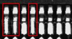 FIGURE 1: Orthogonal view of IC lead coplanarity.
 |
Use of this approach does, however, reach a limit when it comes to fine-pitch ICs without an appropriately adapted pad design, or in the case of micro-bridges. The difference between good and bad cases is hardly distinguishable, as shown in Figures 2A and 2B. Zero-defect inspection is no longer possible. The maximum defect detection rate relative to the number of actual defects is between 50 and 75%, and the pseudo-error rate is also unsatisfactory.
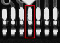 FIGURE 2A: Orthogonal view of a coplanar IC lead without adapted pad design.
 |
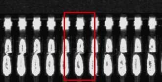 FIGURE 2B: Orthogonal view of a micro-bridge.
 |
Considerably better results are achieved with an inclined camera view, in which – similar to the method used in manual optical inspection – the board is viewed at an angle of 45° to horizontal. The more acute the angle of vision, the less information can be obtained using the inclined view. Figures 3A and 3B depict the same solder joints as Figures 2A and 2B using an inclined camera view.
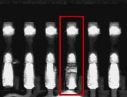 FIGURE 3A: Inclined camera view of a coplanar IC lead without adapted pad design.
 |
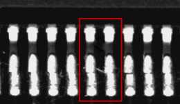 FIGURE 3B: Inclined camera view of a micro-bridge.
 |
The considerably improved optical differentiation between good and bad cases is obvious. And the better one is able to differentiate between good and bad cases, the better the error detection and pseudo error rate become. As in the plain view, switchable lighting permitting different programmable angles of illumination is optimum. Fixed, non-switchable lighting systems do not permit the flexibility required to obtain the best possible contrast for every situation.
As shown in Figures 2A and 2B, solder bridges are situated on the inside between the leads, which are in the shadow in the orthogonal view, making them virtually invisible. The ability to recognize them is considerably better in the inclined camera view.
The use of inclined cameras requires know-how in the fields of calibration and grey scale compensation. If the system is equipped only with an orthogonal camera, the AOI itself does not necessarily have to have the capability of continually monitoring the calibration, as the camera is able to self-calibrate within certain limits. In the case of a multiple camera system, however, the software must enable calibration of the cameras relative to one another and ideally also monitor this beyond the limits of basic calibration. If the software does not permit simple, exact and rapid calibration, the AOI supplier will have problems implementing the integration of the inclined view.
A check on the results is always possible by carrying out a so-called machine capability investigation (MCI). During this procedure, suitable calibration patterns with, for example, 50 runs, are carried out and calculated in accordance with prescribed set values and measuring tolerances (Cm/Cmk values), in which a Gaussian distribution of the measured values is assumed. Whereas Cmk values of >1 have been accepted up to the present (three sigma quality), the trend is toward Cmk >1.67 or even >2 (five or six sigma).
It is clear that in light of these requirements, stable sensory systems are at an advantage. Moveable parts inside the sensor modules tend to degrade precision and reproducibility.
Another skill to be mastered in the use of inclined cameras is compensating for board warpage. This effect causes the solder joint being inspected to “slide” downward in the field of view (Figures 4A and 4B). One method for compensating is to scan the warpage at a sufficient number of points to calculate a model of the warpage. This method, however, adds inspection time. More advantageous is an integrated approach, in which software is used to isolate a larger field of inspection by seeking significant reference points vertically. If appropriate software is available, this method provides reliable results with no additional time.
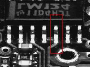 FIGURE 4A: Position of a solder joint without PCB warpage.
 |
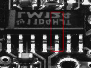 FIGURE 4B: Position of a solder joint with warpage.
 |
Another important criterion in differentiating between AOI systems is camera pixel resolution. With fine-pitch ICs, picture elements of 0.5 mm are normal, as in many designs, the pads and spaces between them each measure 250 µm. If it is necessary to cover the width of the frontal meniscus with at least 15 pixels, the standard resolution of the inclined cameras ought to be well under 20 µm per pixel to obtain images with optimum information content.
A very good camera resolution does require the system performance to be higher, so that AOI does not become a bottleneck on the production line. This applies both to the software (automatic, optimized position generation, use of Traveling Salesman Problem approaches), as well as the camera technology (use of megapixel cameras with a high frame rate) and the positioning technology (high-speed linear drives).
The biggest challenges are in the field of software. Whereas the orthogonal camera view is relatively easy to master, the inclined camera view makes considerably higher mathematical demands on the software development, due of the additional need to differentiate between the angles in the field of view (at least in the four cardinal directions).
In a zero-defect IC inspection strategy, image capture, camera technology and AOI software are the determining criteria of an inspection system. Image capture plays a major role, because only that which “is seen” is available for subsequent evaluation. The orthogonal camera view permits an adequate inspection depth for ICs when the pad design is optimized, although residual escape cannot be completely eliminated, particularly in the case of coplanar IC leads. If the pad design is unoptimized, defect escapes can increase to between 25 and 50%; i.e., detection of the critical types of defects is only 50 to 75%. Due to the small pad sizes, this is not uncommon.
Inclined image acquisition, on the other hand, makes optimum results achievable – even in the case of critical defects. A high-resolution camera with about 15 µm per pixel is well-suited to this task and, in combination with AOI software which clearly contrasts defect characteristics, provides a solid basis for zero-defect IC inspection. New components, such as QFNs, which have space-saving connections both at the side and beneath the component, cannot be adequately inspected orthogonally, and are expected to give inclined camera views a continued advantage.
Peter Krippner is head of the SP division, Viscom AG (viscom.de); (peter.krippner@viscom.de).


Press Releases
- Adam Ryder appointed as Managing Director of Incap UK
- Metal Etch Services Opens New Motor City Facility to Meet Growing Midwest Demand
- Yamaha surface-mount line powers the future of specialized production at Inter-Company in Netherlands
- Matric Group Becomes the First U.S. Manufacturer to Deploy Panasonic NPM-GH Dual Lane SMT Technology