

Toyota Devises Novel Power Electronics Cooling Method
ERLANGER, KY -- A pair of Toyota Motor Engineering & Manufacturing engineers have been issued a US patent for a novel method for cooling power electronics inside printed circuit boards.
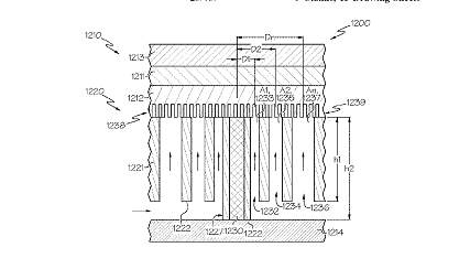
In the filing, Yuji Fukuoka and Ercan Dede describe an electronics assembly that includes a cooling chip structure with a target layer and a jet impingement layer coupled to the target layer. The jet impingement layer has one or more jet channels disposed within the jet impingement layer. Further, one or more through substrate vias are disposed within the jet impingement layer, where the substrate vias are electrically conductive and electrically coupled to the target layer.
A fluid inlet port and a fluid outlet port are fluidly coupled to the one or more jet channels of the jet impingement layer.
The engineers wrote in their application that higher power electronic devices overwhelm conventional heat sinks. The placement and integration of conventional heat sink and cooling structures also present a challenge, they add, and require additional bonding layers and thermal matching materials such as bond layers, substrates thermal interface materials which add "substantial thermal resistance" to the assembly. "Accordingly," they wrote, "a need exists for alternative power electronic assemblies and power electronics devices having cooling structures that also provide electrical interfaces."
The Toyota engineers conceived a pair of alternatives. "In one embodiment, an electronics assembly includes a cooling chip structure having a target layer, a jet impingement layer coupled to the target layer, the jet impingement layer having one or more jet channels disposed within the jet impingement layer, and one or more through substrate vias disposed within the jet impingement layer. The one or more substrate vias are electrically conductive and are electrically coupled to the target layer. The electronics assembly includes a fluid inlet port and a fluid outlet port that are fluidly coupled to the one or more jet channels of the jet impingement layer.
"In another embodiment, an electronics assembly includes a cooling chip structure having, a target layer with a plurality of fins defining a plurality of microchannels. Further, the electronics assembly includes a jet impingement layer coupled to the plurality of fins of the target layer, the jet impingement layer having a plurality of jet channels disposed within the jet impingement layer and a plurality of through substrate vias disposed within the jet impingement layer. The plurality of through substrate vias is electrically conductive and is electrically coupled to the target layer. A first jet channel of the plurality of jet channels is closer to a first through substrate via of the plurality of through substrate vias than a second jet channel of the plurality of jet channels. The first jet channel has a first cross-sectional fluid area that is smaller than a second cross-sectional fluid area of the second jet channel. The electronics assembly includes a fluid inlet port and a fluid outlet port that are fluidly coupled to the plurality of jet channels of the jet impingement layer."
The US patent number is 10566265 and it was issued Feb. 18, 2020.


Press Releases
- Kurtz Ersa Partners with E-tronix for Sales in Illinois and Wisconsin
- XLR8 EMS Welcomes Raul Jorge Lopez Jr. as Director of Program Management and Procurement
- Koh Young America Promotes Ramiro Mora to Lead Service and Applications in Mexico and South America
- ViTrox Americas Welcomes Huy Pham as Technical Support Engineer