

3-D Printing of Plastic Structures onto PCBs for Circuit Protection Strategies
A design, equipment, process and materials methodological approach.
Electronics for automotive applications, as well as for other industries, are expected to reliably operate in harsh environments at a competitive cost. Advances in safety, communication and displays are driving miniaturization and integration of sub-devices onto the PCB assembly; e.g., cameras, sensors, and LEDs. Electrification trends are also leading to higher voltage requirements. In one example of a harsh environment application, automotive door and window control modules may have a critical circuit or component that is desired to function for a specified amount of time, even while submerged in water.
This paper describes an enabling technology to assist in the protection of critical functionality on PCB assemblies. 3-D-printed plastic retaining or "barrier" walls are formed to precisely control the location and height of a dispensed encapsulant in a region of the circuit that is sensitive to the environment. A case study was undertaken for the creation of 3-D-printed retaining walls, formed directly onto the surface of PCB substrates, without the need for separate parts, mold tools, mechanical or liquid fasteners, and complex manufacturing equipment. Also eliminated is the need to encapsulate or pot the entire PCB assembly, which adds additional complexity and cost. The encapsulant-filled retaining wall structure protects critical circuits from chemical, mechanical and electrical external factors such as moisture, fluids, gasses, particulate contamination, physical contact, or arcing in applications requiring high voltage. A 3-D model of the SIR test PCB having a representative retaining wall structure, surrounding an interdigitated test circuit, is shown in FIGURE 1. The retaining walls hold a liquid-dispensed encapsulant in place, at a predetermined height. In the absence of a retaining wall structure, as shown in FIGURES 2 and 3, an encapsulate can spread uncontrollably across the surface of the PCB (Figure 2), or result in insufficient height of the encapsulant, exposing electronics circuitry (Figure 3).
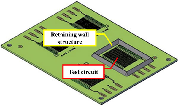
Figure 1. 3-D model of retaining wall on PCB.
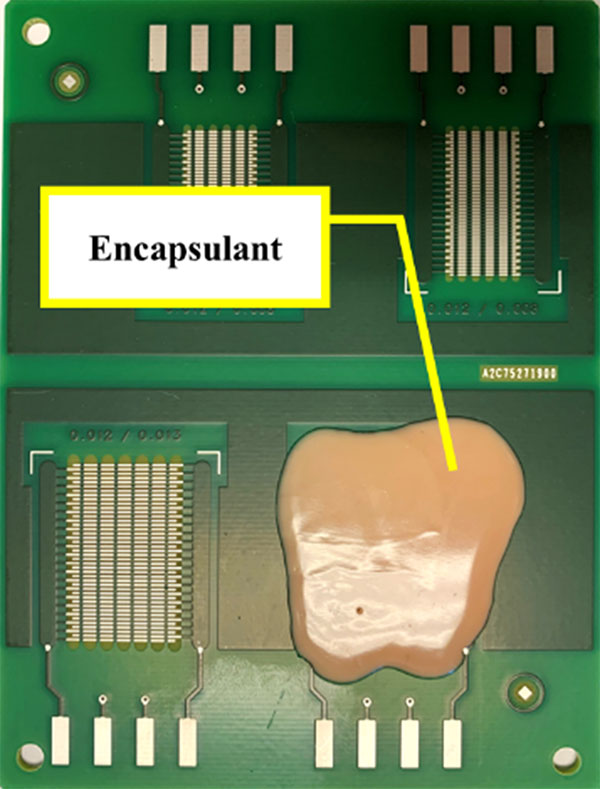
Figure 2. Uncontrolled flow.
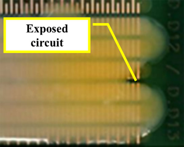
Figure 3. Exposed circuit.
3-D-Printed Retaining Walls vs. Current Practices
A common industry practice for controlling the positioning of an encapsulant on a localized area of a circuit assembly is to first dispense a "dam" material onto the PCB substrate forming the perimeter wall, in a "dam and fill" encapsulation process.1 The dam material is separately dispensed from the encapsulant, or "fill" material, thus requiring additional equipment and manufacturing steps. The dam material may also require a separate cure process and must be chemically compatible with the fill material so as not to interfere with the fill material curing and the final mechanical and electrical properties. Challenges may exist to control the precise height of the liquid-dispensed dam material especially when encapsulating high-profile components. The width of the dam depends on the type of fluid and height. The ratio of the width to the height (i.e., aspect ratio), ranges from about 1.5:1 to 4:1 for different fluids.1 Thus, if one desired to create a liquid-dispensed dam that was 4mm high, the width of the dam would range between 6mm to 16mm, which is an impractical use of PCB surface area for most microelectronics applications. Dam materials also have engineered dispense and thixotropy properties through use of filler additives and controlled molecular weight distributions. Such property manipulations are effective but add to the cost of the dam materials. Some dam and fill processes require a two-step curing process, with the second cure step taking place at 165°C.1 3-D-printed plastics do not require a curing process.
The cost and performance benefits of using 3-D-printed retaining walls for the encapsulation of critical circuits compared to traditional liquid-dispensed dam materials are apparent and can be summarized as: 1) the material cost; e.g., the plastic filaments described in this work cost between $0.025 – $0.035/g compared with the highly engineered liquid-dispense dam materials2, which typically are 30-40 times higher cost; 2) no dedicated liquid-dispense machines are required; 3) cure ovens and curing processes are eliminated; 4) plastic filament materials can be stored at room temperature instead of requiring storage freezers and thawing protocols; 5) there is virtually no process waste of the plastic filaments compared to liquid-dispense materials; 6) material shelf life, handling and inventory control are simplified; 7) a plastic material can be selected that is unreactive to the encapsulant or polymer of interest; 8) the height of the printed retaining wall can be carefully controlled to minimize the amount of encapsulant material required to protect the sensitive circuit; and 9) an "inverted" aspect ratio, e.g., 1:4 (width : height), is theoretically possible for the printed wall, thus conserving PCB surface area compared to the liquid-dispensed dam approach. Such advantages for the 3-D-printed retaining wall approach make it both cost- and performance-attractive.
Alternatively, another current practice for the protection of critical circuits in harsh environments is to conformal coat or pot the PCB assembly. Conformal coatings are generally not considered a suitable protection strategy for fluid-submersion applications in automotive. Potting requires greater volumes of liquid-dispense polymers to protect electronic circuits from the environment when compared to a localized encapsulation design, as the subject of this work. The amount of potting material required depends significantly on the electronic package housing size and geometry, and can easily result in the need for tens or hundreds of grams of potting material to be used, compared with several grams for a localized encapsulation approach. Additionally, potting may present problems for certain types of electronic components that are sensitive to organic contamination, e.g., relays and contacts, or components with solder joints that could be weakened by thermomechanical stress induced by thermal coefficient of expansion effects. A localized encapsulation strategy compared to potting an assembly reduces material usage (read: cost), and avoids risks associated with the thermomechanical stress across a larger PCB assembly.
Scope of this Work
Emerging materials and manufacturing technologies used for additively manufactured electronics (AME)3 and direct digital manufacturing (DDM)4 are leading to exciting breakthroughs in circuit and device designs, as well as process simplifications, that are not possible with 2-D, subtractive PCB manufacturing technologies. The target of this work is of a different nature, instead, to utilize widely accessible FFF printing technology to modify conventional FR-4-based PCBs to add overall PCB assembly and test functionality at a low cost. It was desirable to be able to print the plastic structures within a cycle time comparable to other PCB assembly processes, like a solder reflow process, where thermal profiles take approximately 5 min. to complete.5,6 In this case study, plastic retaining walls were 3-D printed onto IPC-B-24 SIR test PCBs. The artwork of the IPC-B-24 coupon was modified slightly to suit specific materials qualification and application needs (FIGURE 4).7 SIR test boards can be used to perform a myriad of environmental exposure tests on different assembly materials and manufacturing processes.8,9,10 SIR environmental testing itself is not covered here. A 3-D model of the SIR test PCB with the desired retaining wall structure located around an interdigitated test circuit is shown in Figure 1. Although common equipment and materials can be used to 3-D print the retaining walls, considerable process development was required to securely attach the printed plastic retaining walls onto the SIR test PCB. This work describes the methodology and experimental approach leading to the successful creation of 3-D-printed retention walls on FR-4 PCBs.
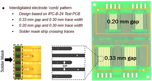
Figure 4. Design of modified IPC-B-24 SIR test board.
Basics of FFF 3-D printers. This work employed fused filament fabrication (FFF) 3-D-printing technology. FFF is a material extrusion technology and is one form of additive manufacturing (AM).11 FFF 3-D printers evolved from filament deposition modeling (FDM) 3-D printers following the expiration of the pioneering patents.12 The basic principles for FFF and FDM technologies are similar. The printing methods employ a plastic filament fed to a heating element by a gear mechanism and then extruded as a melted material from a nozzle onto a print bed or "build plate." FIGURE 5 shows the key components of FFF/FDM printers.13 Typically, the nozzle moves in the x,y-dimensions to form a layer of material. Once this first layer is completed, the plate is lowered in the z-direction, and a second layer is deposited onto the first. Layer by layer, this process is repeated multiple times to complete a three-dimensional print. FFF professional desktop printers are lower cost and have thus gained wider acceptance and use. FFF printer prices usually range in the single digit thousands of dollars and are readily available from a number of companies. FDM/FFF industrial printers are more sophisticated, having more capabilities for print control, and cost in the tens to hundreds of thousands of dollars.11 FFF 3-D printing onto a PCB surface is nontrivial and the experimental methodology will be described in detail below.
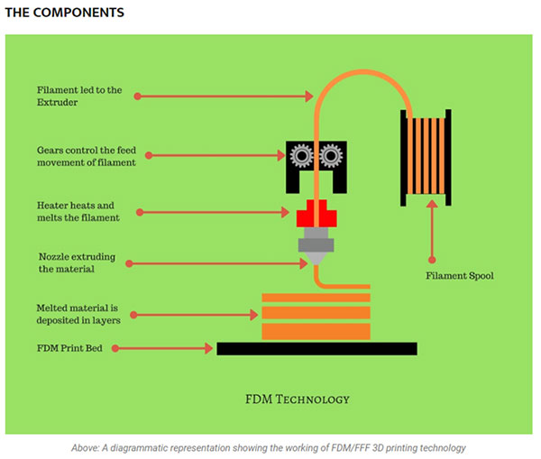
Figure 5. Components of an FDM/FFF 3-D printer.13
Build plates and bed adhesion. The standard approach when creating a 3-D-printed object using FFF is to print, layer by layer, by depositing melted plastic filament starting with the initial layer on the build plate surface (see diagrammatic representation shown in Figure 5). The build plate surface is flat (to maintain a controlled distance to the nozzle), typically made of glass (low cost, readily cleanable), and may be heated. FIGURE 6 shows an example of an FFF-printed object created on a heated glass build plate. Other materials may be employed as build plates provided they are flat and lead to a characteristic called "bed adhesion." Bed adhesion is the ability of 3-D-printed plastic to remain attached to the build plate while printing. Movement of the 3-D-printed object on the build plate surface during the printing process leads to misregistration and scrap. Different build plate materials can be employed to assist with bed adhesion to different plastic filaments. Build plate materials used to establish bed adhesion include aluminum, stainless steel, glass, Kapton tape, PET tape, masking tape and PEI film.14 Other aids can also be applied to a build plate surface to generate bed adhesion including salt-water solution, glue sticks and hair spray. However, someone skilled in the field of SIR testing understands to avoid the use of ionic surface treatments on PCB assemblies for concern of influencing their overall electrical reliability. Generally, heating of the build plate improves the bed adhesion of the melted plastic filament by enhancing wetting and reducing thermal stress between the extruded filament and cooling plastic layers, which can lead to stress-induced warpage and delamination. To summarize, it is important that the build plate surface is flat, has the option for heating, and is compatible with the printed plastic filament to establish sufficient bed adhesion.
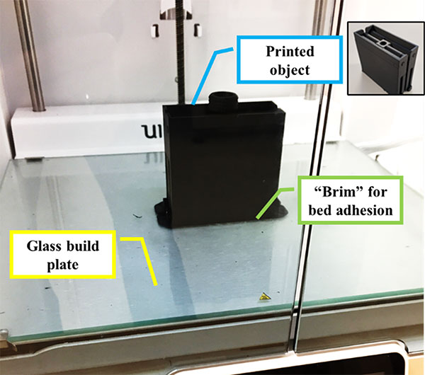
Figure 6. FFF printed object on glass build plate.
Experimental Methodology
Initial attempts at printing onto a PCB. A new aspect of this work compared to the prevailing FFF 3-D-print literature was the desire to print directly onto an FR-4 PCB rather than a traditional build plate. In actuality, the PCB becomes the 3-D-print "substrate," where the desired outcome is permanent attachment of the printed object to the PCB, thus forming a composite structure. This desired outcome varies greatly from traditional FFF 3-D-printing processes in which the object being printed is temporarily fixed to the build plate by bed adhesion for only the duration of the physical printing process. The FR-4 PCBs used for this case study, referred to as "SIR test PCBs" (see Figure 4), were of common construction materials, e.g., epoxy-acrylic solder masks, ImmSn, ENIG, and OSP surface finishes, and 125°C Tg (glass transition temperature) laminates. The initial printed feature attempted was a rectangular prism (FIGURE 7) intended to fully encapsulate one entire interdigitated comb pattern on the SIR test PCBs. Initial attempts to print ABS (acrylonitrile butadiene styrene) filament directly onto the SIR test PCB mounted to the top of the glass build plate resulted in the misprint condition shown in FIGURE 8. First, it was necessary to fix the PCB to the glass build plate with an adhesive, which has the potential to introduce contamination to an SIR test PCB and should be avoided. Second, it was not possible to efficiently transfer heat into the PCB from the heated, glass build plate for the melted ABS filament to wet to the surface of the PCB. Thus, a solution was needed to both firmly position and heat the PCB substrate during printing.
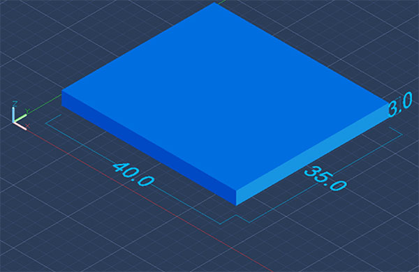
Figure 7. 3-D model, rectangular prism design (mm).
Figure 8. FFF misprint onto PCB using glass build plate.
Custom build plate. A custom build plate was machined from aluminum-2024 having a milled recess or cavity for positioning and retaining the SIR test PCB (FIGURE 9). The aluminum metal also acts to transfer heat to the PCB surface to aid in filament wetting and improving adhesion to the PCB substrate. A thermal interface material may also be placed between the milled recess and PCB to assist in heat transfer to the substrate, if desired. The aluminum build plate could be directly inserted into the commercial 3-D printer. Aluminum-2024 is thermally stable and not prone to warpage. The aluminum plate was compatible with the active leveling program of the 3-D printer, even after 10 cycles. FIGURE 10 shows the SIR test PCB positioned in the recess of the build plate. The 1.6mm thick PCB's surface is flush with the surface of the aluminum build plate. The 3-D-printer's "g-code" (described below in Equipment and Materials Used) was modified with the assistance of the equipment supplier to permit the build plate to remain heated between prints and to bypass the leveling routine. Heating the aluminum build plate to 120°C required 20 min., plus an additional 5 min. to perform the leveling routine. It was possible to bypass heating and leveling in-between prints and reduce downtime when printing on multiple PCBs.
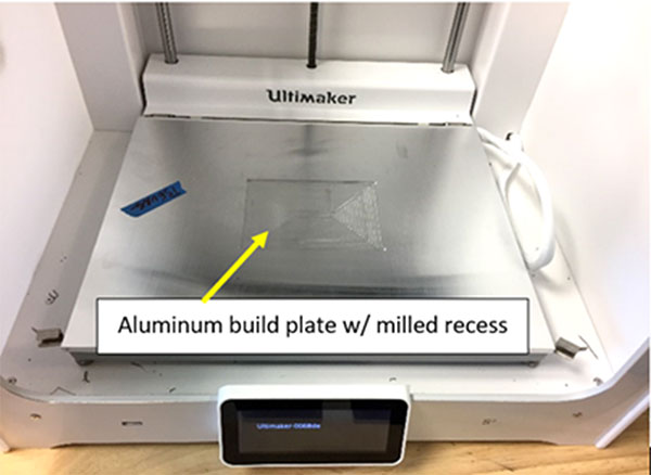
Figure 9. Aluminum build plate with milled recess.
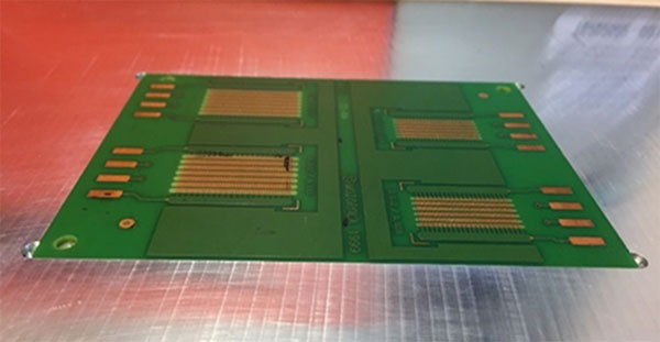
Figure 10. PCB positioned in aluminum build plate.
Design for 3-D printing – the retaining wall structure. The first structure printed onto the PCB using the modified aluminum build plate was a simple rectangular prism (43 x 33 x 3mm) made of ABS plastic (Figure 7). The print process was performed to observe the general adhesion of the material on the SIR comb test pattern. With this structure, the corners of the print contracted and warped (FIGURE 11) as the material cooled. This was observed without and with heating of the build plate at 120˚C. The prism could be printed onto the PCB, but the adhesion was poor due to stress-induced warping.
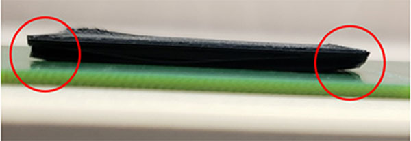
Figure 11. Warping of prism at squared corners.
To reduce the thermal stress on the material, the sharp corners/edges were removed from the original rectangular prism design. Corners were given a small radius, while the sides were tapered (FIGURE 12). With the dimensional changes, the printed ABS filament no longer delaminated from the surface of the PCB. Thus, the thermal stress was reduced, and adhesion was improved.
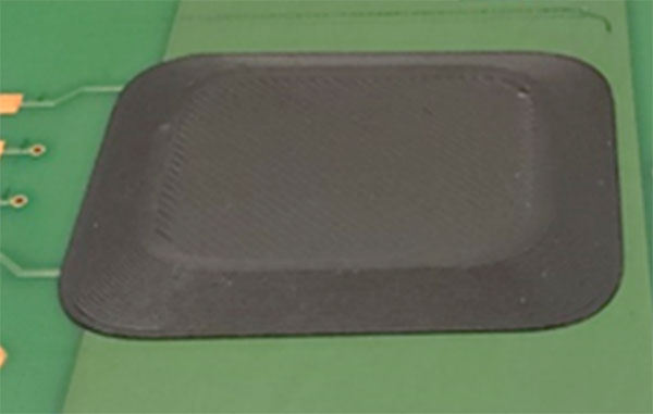
Figure 12. Rounded corners and tapered edges.
A similar design approach to reduce thermal stress was applied to generate the retention walls capable of retaining a liquid encapsulant. In the 3-D model shown in Figure 1, the retaining walls surround the perimeter of the SIR comb test pattern so that liquid encapsulant can easily fill the enclosed area. The dimensions (in mm; see FIGURES 13 and 14) represent a typical area and height that a liquid encapsulant may be required to provide protection for a component or circuit. The wall thickness selected for this case study was 4mm with the tapering angle 56˚ from the horizontal. The corners were rounded with a radius of 2mm to reduce stress on the retaining walls, prevent warping, and improve adhesion of the printed structure to the PCB.
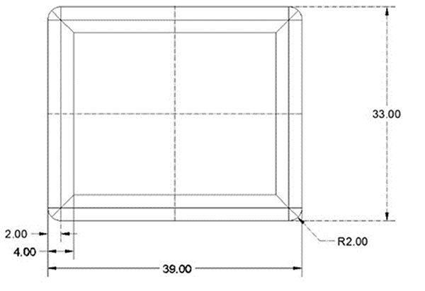
Figure 13. Top view of retaining wall dimensions.
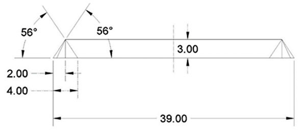
Figure 14. Side view of retaining wall dimensions.
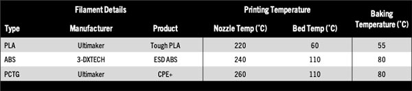
Equipment and materials used. The FFF 3-D printer used for this investigation was a professional desktop Ultimaker S5 open-source printer, which is compatible with third-party plastic filaments. (Au: Note that this work is not a specific endorsement of any 3-D-printer manufacturer. The methodologies described herein are generic and adaptable to various 3-D-printing equipment.) The filaments and their corresponding printing temperature parameters are listed in TABLE 1. Each material was dried at its respective baking temperature for 4 hr. before printing. Three different filament types were selected based on different needs including acceptance in the automotive manufacturing environment, ESD (electrostatic discharge) capability and temperature stability. The x,y,z-resolution of the 3-D printer is specified at 6.9, 6.9 and 2.5µm, respectively. Layer resolution for the 0.8mm nozzle is 20-600µm.
Table 1. Filament Information
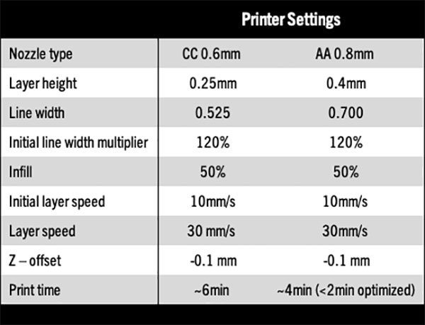
The open-sourced software "Cura" was used to adjust print settings and to slice models. The slicing software slices the object "STL" file (drawing file) to contain the information needed to create a 3-D print.15 The slicing software automatically converts an STL file to g-code. G-code is a widely used computer numerical control programming language in industry and is the language that the printer uses to physically print the 3-D object. The g-code language was modified with the assistance of the printer manufacturer for certain functional aspects described in this work. TABLE 2 lists two sets of parameters used for the prints. The main difference is the diameter size of the nozzle, which directly influences the amount of extruded material. Although there are many settings to consider, the listed settings focus on the condition of the initial layer. The initial layer is critical to establish adhesion or "anchoring" and will be highlighted in the Results section.
Table 2. Printer Settings
Results
For the practical application of the retaining walls diagrammed in Figure 1, it was necessary for the printed walls to form a watertight seal with the surface of the SIR test PCB and to possess sufficient adhesive ability to withstand minor mechanical shocks without experiencing separation from the PCB surface. Several approaches were attempted: Approach I, no surface treatment of the PCB; Approach II, cast-polymer surface treatment of the PCB; Approach III, PCB having milled, thin grooves. The results are described below.
Print approach I: No surface pretreatment of PCB. To establish a baseline for adhesion, ABS filament was printed directly onto the SIR test PCB, which was not modified in any way. This approach resulted in poor adhesion of the printed retention wall structure to the PCB. The structures "popped off" with handling or by minimal force. It was estimated that the shear force to remove the material was <22N (<5lbF). The adhesion was too low to withstand minor mechanical shocks a PCB may experience in common handling. Although no shear force measurements were generated due to the poor adhesion, Approach I will be referred to as the "<22N reference for the PCB non-surface treatment" when comparing with the shear force results from Approaches II and III.
It should be noted that other strategies are widely used in the 3-D-printing field to improve bed adhesion by adding features called "brims."16 A brim is a layer of filament material that extends along the surface of the print bed from the edges of a 3-D-printed object. Brims help to improve bed adhesion and to prevent warping. The printed object is removed from the build plate after the printing process is complete and the brim is mechanically detached. Figure 6 displays an example of an FFF-printed object having a brim to assist with bed adhesion on the glass build plate. Unfortunately, the brim increases the surface area of the 3-D-printed object, which reduces the space available for components mounted to a PCB. Therefore, it was decided to avoid the use of brims on the retaining wall structure. Thus, another approach was desired to improve the adhesion of the printed retaining wall structure to the PCB.
Print approach II: Cast-polymer surface treatment of PCB. The use of "ABS Juice" has been reported in 3-D-print literature to pretreat the surface of glass build plates to improve bed adhesion and reduce warping of the printed object.17 ABS Juice is dissolved ABS filament in acetone solvent and the procedure for its preparation is described in the corresponding reference. Generally, the ABS Juice is brushed onto the glass bed while hot and the acetone evaporates, leaving a thin cast film of ABS coating the build plate. To improve adhesion of the initial layer of printed ABS on the SIR test PCB, ABS Juice was prepared and brushed as a thin coating onto the PCB surface around the border of the interdigitated comb pattern where the ABS retaining walls will be printed. The ABS Juice was allowed to dry for 1 hr. at 25°C and then heated on the build plate at 100°C for 10 min. The acetone evaporated as the thin coating was heated, leaving a layer of ABS (FIGURE 15). The deposited or "cast" ABS polymer layer acted as a foundation for the 3-D printer to print the ABS retaining walls. The printed retaining walls had greater adhesion than with no surface treatment of the PCB and could be measured using an Instron. The shear test configuration used to measure the push off force of the retaining wall frame structures is shown in FIGURE 16. The SIR test PCB was held on the bottom side in a vise and a chisel tool was used to push on one wall of the printed retaining wall from the top direction. The crosshead speed used for the shear test was 10mm/min. With the addition of the ABS Juice surface pretreatment, the average shear force to push off the printed ABS retaining walls increased to an average of 49N (FIGURE 17, orange dots indicate maximum shear forces at failure), compared to the <22N reference for the PCB non-surface treatment approach (red-dashed line).
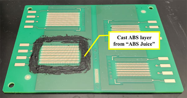
Figure 15. ABS layer cast around comb pattern.
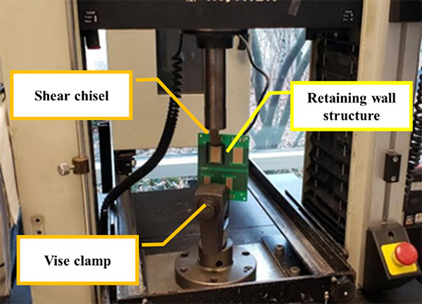
Figure 16. Instron setup for shear test.
The ABS Juice or cast polymer surface preparation method enhanced the adhesion of the ABS printed retaining walls to the point where the PCB composite structures could be handled carefully and remain intact. Note, however, that it is nonideal to use the solvent mixture to prepare the PCB surface for 3-D printing. Control of the applied ABS Juice is not precise and the solvent itself may result in adverse reactions hindering circuit reliability. Additionally, more aggressive solvents may be necessary depending on the type of plastic filament used to generate the cast polymer layer. Thus, another approach was desired to improve the structural adhesion of the printed retention walls other than polymer casting.
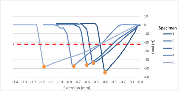
Figure 17. Shear force of ABS wall structure after pretreatment of PCB surface with ABS Juice.
Print approach III: PCB having milled, thin grooves. The next, and ultimately successful approach, was to enable mechanical adhesion or mechanical anchoring by physically modifying the PCB. The perimeter of the comb pattern was milled to create thin grooves on three sides of the PCB comb pattern (FIGURES 18 to 20). The grooves have a width of 0.8mm and a depth of 1.0mm. One side of the comb pattern was not milled to preserve the copper signal traces for SIR test measurements. Future work will place the signal traces on the opposite side of the PCB and use conductive vias to route to the comb test pattern. The 1.0mm deep milled grooves do not extend all the way through the 1.6mm thickness of the PCB and it is still possible to route traces under the milled grooves. The grooves can be created at the PCB suppliers' factories at the same time the standard routing and milling operations are performed. Thus, no secondary milling operation of the PCB would be required as was performed for this work.
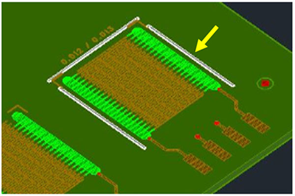
Figure 18. Drawing of milled grooves in PCB.
The FFF 3-D-printed filament was extruded into the milled grooves, using the printer parameters listed in Table 2, creating additional points of mechanical "lock & key," or anchoring within the PCB epoxy-glass laminate region. The possibility also exists for improved adhesion through attractive molecular forces of the glass fiber surface and the printed plastic. To fill the milled grooves, it was necessary to modify the g-code language and enable the printer to print with a negative z-offset over the grooves. Typically, there is a minimum z-offset to prevent the nozzle from impacting the build plate while printing, thus protecting the equipment. The negative z-offset setting was added to change the distance between the nozzle and the build plate. This permitted the nozzle to sit flush against the PCB grooves.
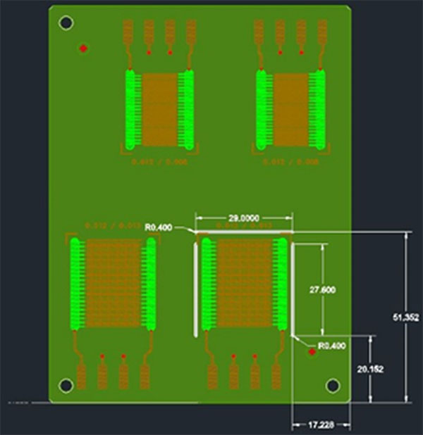
Figure 19. Groove dimensions, 0.8mm W x 1.0mm D.
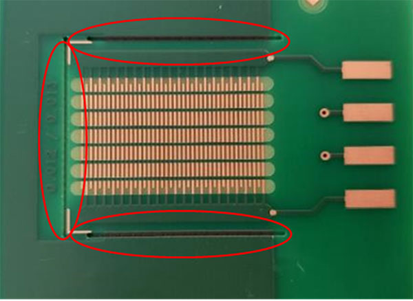
Figure 20. Milled grooves in PCB for anchoring.
In addition to the print parameters listed in Table 2, the ratio of extrusion nozzle diameter to the groove width is important for maximizing structural adhesion. Printing with a 0.6mm diameter nozzle into a 0.8mm groove yields the shear force data shown in FIGURE 21. As can be observed, the average shear retention force is increased to 111N (see orange dots for maximum shear forces at failure) using the milled, thin grooves. This compares to the approximately 49N for the ABS/acetone PCB pretreatment method shown in Figure 17 and the <22N reference for the PCB non-surface treatment approach (red-dashed line). There is a notable amount of variance between test specimens, however.
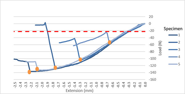
Figure 21. Shear force of ABS wall structure with PCB grooves; 0.6mm diameter extrusion nozzle.
When examining the underside of the removed printed retaining walls, it was observed that the ABS filament did not completely extrude and fill the grooves, see FIGURE 22. The incomplete filling of the grooves with ABS using the 0.6mm nozzle was believed to be a contributing factor behind the force variations observed in the shear data shown in Figure 21.
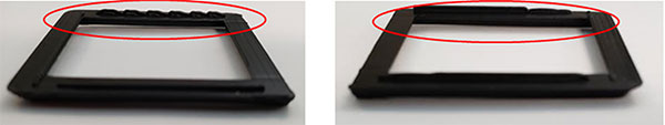
Figure 22. Removed retaining wall structures showing incomplete ABS extrusion into 0.8mm PCB grooves using 0.6mm diameter nozzle.
To maximize the potential benefits of the grooves for mechanical anchoring, additional PCB composite structures were printed using a 0.8mm diameter extrusion nozzle that matched the width of the PCB grooves. Printer variables including z-offset and print speed were held constant. FIGURE 23 shows the 0.8mm diameter nozzle together with ABS filament gave consistent and higher shear force values, exceeding 133N, compared to the <22N reference for the PCB non-surface treatment approach (red-dashed line). The shear values would be even greater, but the plastic material itself deformed and cracked during the shear testing (FIGURE 24). The mechanical anchoring ability of the groove features exceeded the strength of the ABS plastic walls. Please also note that the Instron chisel applied the push-off force directly to the one wall of the printed retaining wall frame that was not anchored by the milled grooves – i.e., the weakest of the four walls of the printed retaining wall structure – thus producing the worst-case shear result for the printed retaining wall structure.
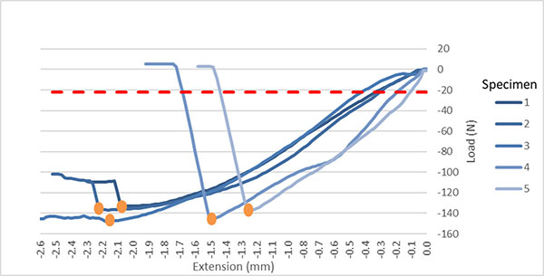
Figure 23. Shear force of ABS wall structure with PCB grooves; 0.8mm diameter extrusion nozzle.
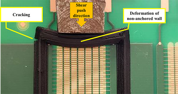
Figure 24. Deformation and cracking of ABS wall structure during Shear due to superior mechanical anchoring of filled 0.8mm grooves. Specimen printed using 0.8mm diameter extrusion nozzle.
Inspection of the removed retaining wall structure shown in FIGURE 25 revealed that the PCB grooves had filled completely when using the 0.8mm diameter extrusion nozzle along with the same z-offset and print speed as used for the 0.6mm nozzle. Thus, matching the nozzle diameter with the PCB groove width is an important design-for-print parameter for creating robust PCB composite structures. The variance observed in the shear data for the 0.6mm diameter nozzle was no longer observed with the 0.8mm nozzle, thus confirming that the complete filling of the grooves with plastic is important to establish consistent anchoring strength. The 0.8mm width PCB groove/0.8mm diameter extrusion nozzle, along with the process parameters listed in Table 2, and the wall design features described in Figures 13 and 14, yielded a 3-D-printed, ABS retaining wall/PCB composite structure that could be securely handled for additional processing and testing.
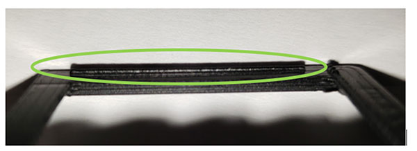
Figure 25. Removed wall structure showing full ABS filling of 0.8mm PCB grooves using 0.8mm diameter extrusion nozzle and parameters in Table 2.
The following investigations examined different plastic filament materials by applying the optimized 0.8mm diameter nozzle parameters from Table 2.
Plastic filament materials evaluated. As mentioned in Experimental Methodology, three different plastic filament materials were evaluated based on different needs: 1) acceptance in the automotive manufacturing environment, 2) ESD capability, and 3) temperature stability. All work described thus far has been with the ABS filament listed in Table 1. ABS filament is generally used for applications where strength, ductility, machinability, and thermal stability (95°C) are required. The ABS filament used for this work has an additional characteristic of being an ESD-safe filament, formulated for applications that require ESD protection. ESD protection is a general concern with the handling of electronics devices and the ESD-safe filament was thus evaluated. In addition to ABS, the FFF filaments "Tough PLA" (polylactic acid) and PCTG "CPE+" (polycyclohexylenedimethylene terephthalate glycol-modified) were also evaluated. PLA is a vegetable-based, renewable-source plastic. PCTG is a derivative of the PETG plastic category. PCTG is known for its toughness, wear, chemical, and temperature resistance (100°C vs. 60°C for PLA). The same design-for-print methodology that had been implemented for the ABS filament (Table 2; 0.8mm diameter nozzle), was utilized for the PLA and PETG filaments to demonstrate whether the success described above for the ABS filament could be expanded to different filament materials.
The shear force data presented in FIGURE 26 are for the printed PLA filament and in FIGURE 27 for the printed PCTG filament. Unlike the ABS printed retaining wall/PCB composite structures, the PLA and PCTG printed retaining walls did not detach from the PCB during shear test. Instead, the retaining walls remained anchored in place, while the material deformed from the applied force of the Instron chisel. This observation was reflected within the shear force graphs – showing no instantaneous change in load indicative of a sudden separation. For this reason, these graphs are more representative of the material strengths of the PLA and PCTG filaments rather than their ability to remain mechanically anchored to the PCBs. The PLA retaining walls deformed at an average force of 165N as shown in Figure 26 vs. the <22N reference for the PCB non-surface treatment approach (red-dashed line). The PCTG retaining walls deformed at a lower applied shear load than with the PLA.
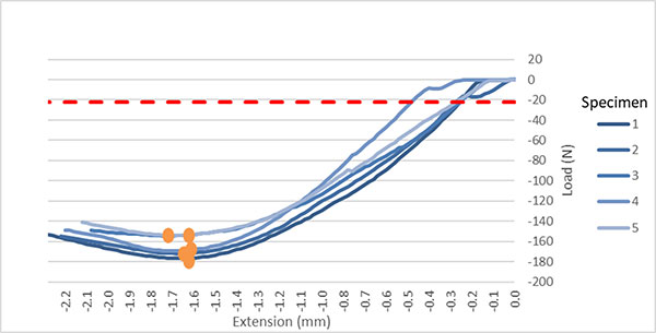
Figure 26. Shear force of PLA wall structure with PCB grooves; 0.8mm diameter extrusion nozzle.
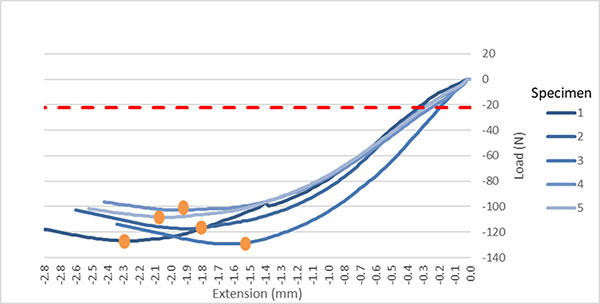
Figure 27. Shear force of PCTG wall structure with PCB grooves; 0.8mm diameter extrusion nozzle.
Figure 27 shows that the 0.8mm nozzle together with PCTG filament also gave very consistent shear values, 102-133N vs. the <22N reference for the PCB non-surface treatment approach (red-dashed line). The PCTG has higher temperature stability, and is also flexible, so the shear force data are not indicative of any loss of the mechanical anchoring adhesion of the PCTG to the milled PCB grooves, but rather the values are representative of the deformation of the PCTG plastic material itself. The 0.8mm width PCB groove printed with the 0.8mm diameter extrusion nozzle, along with the process parameters listed in Table 2, and the wall design features described in Figures 13 and 14, yielded 3-D-printed, PLA and PCTG retaining wall/PCB composite structures that could be securely handled for additional processing and testing.
3-D-print process time required to create the retaining wall structures. It was desirable to print the plastic structures within a cycle time comparable to other PCB assembly processes, such as a solder reflow process, where thermal profiles take approximately 5 min. With basic printer and software optimization enhancements, the retention walls were printed in under 2 min., using PCTG filament and the 0.8mm diameter nozzle, thus enabling the possibility of volume scalability. Extrusion of melted plastic into the milled groove is a key step requiring adherence to the parameters listed in Table 2 but the time required for printing the remaining retaining wall structure can be further optimized by employing additional print speed, layer height, infill pattern, and shell strategies with the slicing software.18 There was a general concern that further effort to reduce print time could impact the print quality and mechanical properties of the retaining wall and the time limits were not pushed any further. 3-D printers and materials are experiencing rapid advancements which should lead to the possibility of further cycle time reductions in the future without a significant impact to quality.
Retaining wall / SIR test PCB composite structures filled with a liquid-dispensed encapsulant. FIGURE 28 shows the PCTG printed retaining walls on the SIR Test PCB following extrusion into the fine grooves. The mechanical anchoring strength was greatly enhanced by the milled, thin groove features as demonstrated in the Figure 27 shear data. FIGURE 29 shows the encapsulant-filled, PCTG printed retaining walls. FIGURE 30 is a magnified view of the encapsulated comb circuit on the SIR test PCB. FIGURE 31 shows the PCTG printed retaining wall composite structure's ability to create a watertight seal to the PCB surface.
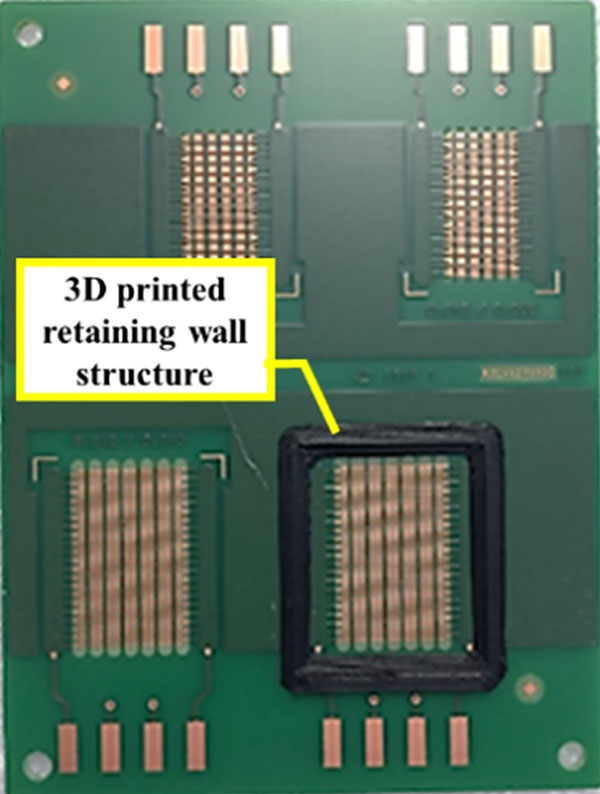
Figure 28. PCTG retaining wall on SIR test PCB.
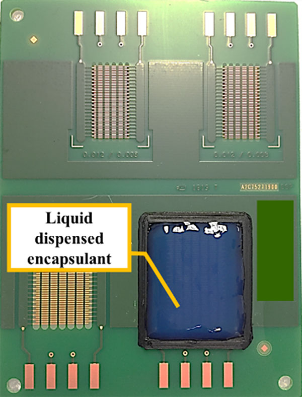
Figure 29. Encapsulated SIR test PCB circuit.
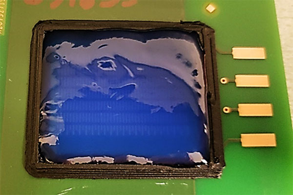
Figure 30. Magnified retaining wall with encapsulant.
Heat treatment impact on 3-D-printed, plastic/PCB composite structures. The impact of post-print heating on the adhesion of PCB composite structures was also investigated. Some liquid-dispensed encapsulants require heating to cure. To investigate the impact of temperature on adhesion of the printed structure, the PCTG/PCB composite structures were heated to 100°C for 1 hr. Next, the PCBs were cooled to room temperature and the shear force evaluated in the same manner as the printed retaining walls without the post-heat treatment. As observed in FIGURE 32, the shear force values were consistent and ranged between 111-133N, indicating no degradation in adhesion of the PCTG printed wall structures occurred due to thermal exposure when compared to the non-heat-treatment shear values in Figure 27. Once again, the red-dashed line represents the <22N reference for the PCB non-surface treatment approach.
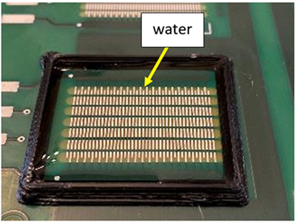
Figure 31. PCTG wall retaining water.
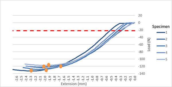
Figure 32. Shear force of PCTG wall structure with PCB grooves; 0.8mm dia. nozzle; exposure to 100⁰C for 1 hr.
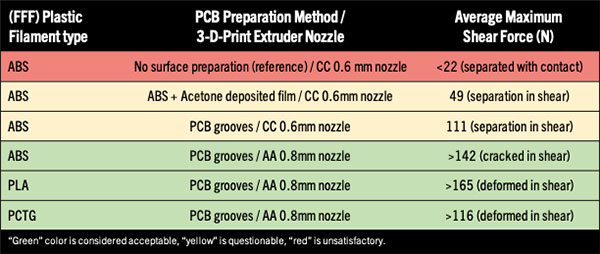
The shear force adhesion data reported above are summarized and compared in TABLE 3. Note that printing into the milled, thin grooves of the PCB substrate provided excellent anchoring of the 3-D retaining wall structure for the three types of plastic filaments evaluated: ABS, PLA and PCTG. The plastic materials themselves cracked or deformed before the retaining wall structure detached from the PCB. The printed retaining wall/PCB composite structures could be handled normally during dispense and cure operations, with no separation of the retaining wall structures from the PCBs.
Table 3. Summary of Retaining Wall Structure Shear Test Results Based on Different Factors
Discussion
This article details a methodical experimental approach that ultimately led to the appropriate design, equipment, process, and material parameters required for the successful formation of 3-D-printed plastic/PCB composite retention wall structures.19 The key parameters are summarized in this section.
FFF 3-D printer physical modifications. A conventional, desktop FFF 3-D printer was used and described herein. Professional desktop FFF printers are relatively low cost, ubiquitous in industry, and some offer open-source materials and software usage, which permit expanded development opportunities. However, in a paradigm shift from routine FFF 3-D-printing work, where objects are created layer-by-layer on the build plate and then removed afterward as a finished or semifinished part, the intention of this work was to create a structurally anchored object onto a PCB as a permanent composite structure. It was found that attaching a PCB to a conventional glass build plate led to a misprinted object due to insufficient "bed adhesion" to the PCB substrate. An aluminum build plate was developed (Figure 9), having a milled recess and specific dimensions to fix the PCB in the x,y-direction and flush with the aluminum build plate surface in the z-direction (Figure 10). Heat transfer to the PCB surface was improved and the PCB could be held in position without tape or fasteners. The modified aluminum build plate was inserted into the 3-D printer, replacing the glass build plate. Printing objects onto the "as received" PCBs was made possible with the aluminum build plate, albeit with limited adhesion initially due to thermal stress (Figure 11).
Design for stress reduction in retaining wall structure. One aspect for improving adhesion between the 3-D-printed retaining walls and PCBs was to maintain thermal stress to a minimum. Thermal stress leads to warping and often delamination from the build surface. To minimize stress, rounded corners and tapered edges were incorporated into the retaining wall design as described in Figures 12-14. The stress-minimized design led to a PCB printed structure without warping but adhesion was still not suitable for handling purposes.
Design of milled, fine grooves in PCB surface. The creation of milled, thin grooves (0.8mm width x 1.0mm depth) into the PCB surface, where 3-D printing of filament was possible, ultimately led to the robust mechanical anchoring, and water tightness, of the 3-D-printed retaining wall structure to the PCB. The milled, thin grooves are shown in Figures 18-20. The grooves did not extend through the entire thickness of the PCB (1.6mm PCB thickness vs. 1.0mm groove depth), thus leaving the possibility to route conductor traces opposite the thin grooves. The fine grooves were milled in-house but could also be created at the PCB manufacturers during standard routing operations. The grooves were not created where copper signal traces were present to allow for electrical testing. Future SIR test PCB designs will route the copper signal traces in a manner to permit groove formation on the full perimeter of the test circuit. Nevertheless, having grooves anchoring three of the four walls of the retaining wall structure was sufficient to produce secure handling and processability along with encapsulant (Figure 30) and water tightness (Figure 31). The effective mechanical anchoring of the 3-D-printed filaments to the PCB milled grooves required additional process development and minor software modifications discussed below.
Print parameters and printing time. The print parameters for the key initial print layer, required to fill the groves, are summarized in Table 2. Minor manipulation of the printer's g-code language was required to enable a negative z-offset print direction to fill the milled grooves on the PCB. Also important was to match the nozzle diameter with the groove width, at 0.8mm, in order to achieve complete fill of the grooves (see Figures 22 and 25). The time required for printing the retaining wall structure was optimized to under 2 min. without any rigorous effort invested to reduce the overall print time. The printer's g-code language was also modified to enable continuous heating and leveling of the aluminum build plate to eliminate downtime between prints. A print time of under 2 min. is comparable to other electronics manufacturing processes such as reflow soldering, which takes approximately 5 min. Additional print time reductions are possible by employing print speed, layer height, infill pattern, and shell strategies with the slicing software. Thus, high-volume scalability of 3-D-printed/PCB composite structures is possible under the appropriate circumstances. Additionally, 3-D-printer technologies including print capability and materials are developing rapidly and greater efficiencies are likely to be realized in the future.
Overall effectiveness and adaptability of the milled, thin PCB grooves and print parameters with different filaments. The effectiveness of the milled, thin PCB grooves, in combination with the print parameter development, in establishing mechanical anchoring adhesion, was demonstrated with three different filament materials, ABS, PLA and PCTG (see Figures 23, 26, and 27). The 0.8mm width PCB groove printed with the 0.8mm diameter extrusion nozzle, along with the process parameters listed in Table 2, and the wall design features described in Figures 13 and 14, yielded 3-D-printed ABS, PLA, and PCTG retaining wall/PCB composite structures that could be securely handled for additional processing and testing. The retention walls also maintained their adhesion during a subsequent heating process (representing the encapsulant cure). As summarized in Table 3, the three different filaments evaluated gave excellent anchoring adhesion that exceeded the inherent mechanical strength of the printed plastic materials themselves. The height of the retaining wall structures in this work was 3mm but could be made higher or lower depending on the circuit or component that requires encapsulant protection. The approach described in this case study to create 3-D-printed/PCB composite structures could be widely applicable to other designs, applications, and materials.
The encapsulant-filled retaining wall structures can assist to protect critical circuits from chemical, mechanical and electrical external factors like moisture, fluids, gasses, particulate contamination, physical contact or arcing in applications requiring high voltage. The retaining walls can be designed and printed to almost unlimited geometries and shapes to optimize the amount of protective material used and to protect varying topographies of devices and circuits. The SIR test PCB described in this work can be used as a basis to evaluate a myriad of encapsulants and polymeric materials under different environmental conditions. Similar design, process, and materials principles described in this work to create the 3-D-printed retention walls on an IPC-B-24 style test PCBs could also be considered for populated test assemblies like the IPC-B-52 test assembly.20
Conclusions
This paper presented the novel case study of using FFF 3-D printing to extrude melted plastic filament directly into thin grooves formed on a conventional PCB thereby creating mechanical anchoring adhesion from which to print retaining walls for the location-controlled encapsulation of critical circuits. Newly described in this work, 1) a 3-D-printer build plate, having a dimensionally specified recess, was developed using aluminum to fix and heat the surface of the PCB substrate, 2) an FR-4 PCB was used as a 3-D-print substrate to create a composite plastic structure, 3) plastic retention wall design features were developed to minimize thermal stress, 4) thin grooves were milled into the PCB surface and used to anchor the printed filament, 5) the 3-D-print dispense nozzle diameter was optimized to the width of the PCB milled groove and 6) 3-D-print process parameters were developed to ensure complete filling of the grooves during the first print pass. The design, process, and material parameters were detailed. Only minor modifications of the printer's g-code language were required to ensure filling of the thin milled grooves and to reduce downtime in-between prints that would have been caused by the re-heating of the aluminum build plate. The approach and methodology are flexible and adaptable and can be applied to the creation of other new 3-D-printed plastic/PCB composite structures. The equipment and materials used to create the 3-D-printed retention walls are low cost, readily available, and required only minor modifications. The 3-D-print time, under 2 min., is comparable to other typical manufacturing processes like reflow soldering and has the potential for volume scalability. The 3-D-printed retaining walls created on SIR test PCBs can be used to develop circuit protection strategies for products operating in harsh environments such as Automotive.
Acknowledgments
The authors would like to thank Jeremy Simon for helpful discussions on the printer's g-code and how it could be adjusted for certain aspects of this work, as described in the paper.
This article is adapted from a paper titled "3-D Printing of Plastic Structures onto PCBs for Circuit Protection Strategies" and was first presented at the 2023 IPC Apex Expo Technical Conference, with original work published within conference proceedings.
References
1. S.J. Adamson and C.Q. Ness, "Dam and Fill Encapsulation for Microelectronic Packages," Proceedings of Nepcon West, February 1999.
2. J. Flynt, "How Much Does 3-D Printing Filament Cost?" 3-D Insider, Sept. 10, 2017.
3. J. Nulman, "Advances in Multi-level and Multi-material Additively Manufactured Electronic (AME) Circuits and Devices," Proceedings of IPC Apex Expo, January 2022.
4. J. Benoit, N. Willey, J. Goldfarb and K. Church, "Conformal Printed Circuit Structures," Proceedings of IPC Apex Expo, January 2022.
5. J.H. Lau, C.P. Wong, N.C. Lee and S.W.R. Lee, Electronics Manufacturing with Lead-Free, Halogen-Free, & Conductive-Adhesive Materials, McGraw-Hill, chapter 15, 2003.
6. IPC, IPC-7801, Reflow Oven Process Control Standard, section 4, March 2015.
7. L.C. Cohen and S.F. Rak, "SIR Test Method for Underfill Reliability in Automotive Electronics," IPC Electronics Materials Forum, Nov. 5, 2019.
8. IPC, IPC-9201A, Surface Insulation Resistance Handbook, August 2007.
9. IPC, IPC-TM-650, Test Methods Manual, Surface Insulation Resistance, method 2.6.3.7.
10. K. Bawagan, C.M. Pamatmat and S.F. Rak, "Surface Insulation Resistance (SIR) Test for Raw Material Release," IPC WorksAsia and Automotive Electronics Reliability Conference, Jun. 23, 2017.
11. BCN3-D Technologies, Inc., Introduction to Fused Filament Fabrication (FFF) 3-D Printing Technology, WH-03-EN-v1.2, 2019.
12. G. Khanolkar, "Difference between FDM and FFF Technologies," Mar. 15, 2018, https://blogs.truventor.ai.
13. Manufactur3-D, "How Does the FDM 3-D Printing Technology Work?" Manufactur3-D Magazine, Jan. 29, 2018.
14. B. Goldschmidt, "3-D Printer Bed Adhesion: All You Need to Know," All3-DP, Jun. 26, 2022.
15. Ultimaker "Cura" is a free 3-D printing software at ultimaker.com. It can be integrated with CAD software or customized.
16. A. Chavan, "3-D Printing Brim: When Should You Use It," All3-DP, Jul. 11, 2018.
17. MatterHackers (2015, December 18). ABS Bed Adhesion Tips & Tricks, www.matterhackers.com.
18. O'Connell, J. (2021, May 6) Fast 3-D Prints: How to Increase Your 3-D Printing Speed, All3-DP, www.all3dp.com.
19. S.F. Rak and D. Tseung, Sept. 10, 2021, patent pending.
20. IPC, IPC-9202, Material and Process Characterization/Qualification Test Protocol for Assessing Electrochemical Performance, October 2011.
is the Principal at S.F. Rak Company, specializing in materials science and electronics manufacturing consulting for the automotive industry. Previously, he worked 29 years combined at Continental Automotive and Motorola Automotive Group in global, manufacturing technology roles. Rak has a doctorate in organic chemistry from the University of Minnesota; stanton@sfrak.com. is a production engineer at Nouryon. He has a bachelor's in chemical engineering from Illinois Institute of Technology.
PCB West, Engineering Tomorrow’s Electronics / September 19-22, 2023


Press Releases
- Adam Ryder appointed as Managing Director of Incap UK
- Metal Etch Services Opens New Motor City Facility to Meet Growing Midwest Demand
- Yamaha surface-mount line powers the future of specialized production at Inter-Company in Netherlands
- Matric Group Becomes the First U.S. Manufacturer to Deploy Panasonic NPM-GH Dual Lane SMT Technology