

Cell Metallization Alternatives to Screen Printing
Several noncontact methods exist, but are they practical?
As a researcher and proponent of screen-printing technology (and, of course, an employee of one of the world’s top mass-imaging organizations), you may find it strange that I’m writing about alternative solar cell metallization technologies. But these other approaches do exist, and it’s important to understand them – and why many experts with no vested interest in screen printing still view the latter as the most viable, at least for the medium-term future.
Many alternative techniques have been around for a few years, and concurrent with their development has been the claim that one or more would displace screen printing as the reigning technology. So far that hasn’t happened, for two reasons: 1) Printer and paste manufacturers have kept pace with the latest demands for fine-line printing (we’re now sitting at 60µm wide lines in production and well below 50µm in a lab environment); and 2) the requirement for much thinner silicon (which would be subject to potential damage by the contact of printing’s squeegee pressure) to reduce cost has diminished in recent years, as the price of silicon has gone down by more than half.
Generally, the alternative metallization methods described below were applied to solar to reduce costs or to increase efficiency. In some cases, this was largely driven by the need to deposit material in a noncontact process to enable thinner silicon use. Each has its perceived advantages compared to screen printing (primarily noncontact techniques), as well as its drawbacks.
Laser transfer printing. This is a noncontact technology that uses a continuous tape loop and doctor blade arrangement to deposit paste, then locally heat the paste with a laser, which ejects the paste from the tape onto the wafer. Although nothing touches the wafer and the consumables costs are relatively low, this method cannot currently produce fine lines in high-volume manufacturing, and, consequently, the only viable market for it is for printing the back side of solar cells. Throughput is also fairly low.
Electroplating. This process – used also in semiconductor and printed circuit board fabrication – employs a chemical method to remove the silicon nitride locally, plate with a material (likely electroless nickel) to make the first contact with the wafer and electroplate the bulk copper on top of that. Because of copper’s corrosion problem, it then has to be passivated with a tin layer. The advantages of electroplating are the ability to produce ultra-fine lines with high conductivity and eliminate costly silver pastes. However, it does require three wet chemical processes that are time-consuming, labor-intensive, messy and waste-producing. This method also requires fairly high skills.
Seed print and light-induced plating. Either a screen- or an inkjet-printed low aspect ratio line is deposited with standard silver paste, and then silver is electroplated using the current generated by the cell itself during light exposure. In my view, the benefits of this technique are quite limited; there is a bit of extra conductivity from the silver because the electroplated silver is solid (as opposed to the honeycomb effect of fired silver paste), and there is reduced shadowing from the ability to plate narrow lines. But, the lines are limited to 50/60µm widths, which can be achieved already with screen printing. The disadvantages of a two-stage process, the additional capital expenditure for plating equipment, the line width limitations, and the chemical waste outweigh the marginal benefits.
Inkjet printing. This technology has been around for a long time and has various commercial applications. Initially, advocates thought it would be ideal for noncontact solar cell printing because of the historic success with inkjetting materials. But, inkjet printing requires low viscosity materials with nano-particles, so the paste is more expensive than traditional silver paste. Plus, most inkjet systems are challenged by high aspect ratio printing and need 10 to 20 passes to get the required height. The multiple passes obviously lower throughput significantly. There are also nozzle blockage issues. All in all, I think it’s very impractical for solar cell processing.
Aerosol or metal jetting. With aerosol or metal jetting, material is guided by pressurized gas and deposited onto the substrate. This method is noncontact, can do ultra-fine lines and has the positional accuracy of deposition. However, like inkjet printing, it is plagued by its inability to deliver high aspect ratios at high speed and also requires special inks.
Dispensing or extrusion. Automatic dispensing (also referred to as extrusion in some cases) for solar cell metallization is not that different from what is commonly used in electronics assembly. This is a needle dispensing technique where pastes are transferred in a non-contact method from the nozzle to the substrate. Dispensing is capable of achieving high aspect ratio line widths of 50µm, with further reductions likely, and has good positional accuracy. The drawbacks include the required use of special (read: expensive) pastes, nozzle blockage and low throughput.
Laser chemical metal deposition. Largely an experimental technique, laser chemical metal deposition is likely a few years away from any sort of commercialization. With this process, the solar cell is immersed in an electrolyte; a laser shines through the electrolyte, ablates an anti-reflective coating and causes activity in the emitter layer, which electroplates nickel lines. The advantages are its noncontact capability and the elimination of silver. If and when it becomes commercially viable, these advantages will have to be weighed against the associated waste, health and safety issues of a wet process.
Sputtering or evaporation. These technologies have been used in the semiconductor industry for a long time. Because they are semiconductor-accurate, extraordinarily fine lines and high aspect ratios can be achieved in a noncontact process. What’s more, just about any metal or stack of metals can be deposited. On the downside, sputtering and evaporation are very slow and require a high vacuum process. Throughput is adversely impacted by the requirement to have everything go through a vacuum chamber first. There are also tooling costs associated with making the photolithography resists used to define the plated or metal-coated areas. If this is achieved through a mask, then that is a tooling cost as well. Currently, the capital expenditure costs are high, but there is industry chatter about these techniques becoming more useful for backside aluminum.
So, there you have it: the pros and cons of screen printing alternatives to solar cell metallization. Currently, there is no other method that can deliver the aspect ratio or speed efficiency of screen printing. The technology’s inability to offer noncontact material deposition seems to be a moot point, if and until silicon wafer thickness begins to diminish. Even then, modern printing systems can effectively manage wafers as thin as 120µm with very low breakage rates. And while printing can’t eliminate silver pastes until there are fully functional, commercially available non-silver pastes, it can assist with reductions in silver consumption right now. Using print-on-print (POP) and dual print technologies, the cost impact of silver can be significantly mitigated. (“Strategies to Offset the Rising Cost of Silver,” "CIRCUITS ASSEMBLY, September 2011.) For the time being, I am of the firm opinion that screen printing is the most cost-effective, efficient method available for solar cell metallization.
[Ed.: To enlarge the table, right-click on it, then click View Image, then left-click on the table.)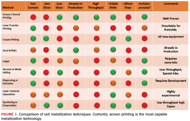
Tom Falcon is a senior process development specialist at DEK Solar (dek.com); tfalcon@dek.com. His column runs bimonthly.


Press Releases
- Javad EMS Upgrades Through-Hole Soldering Capacity with New SEHO PowerWave System
- Sharpen Your Selective Soldering Skills with Kurtz Ersa's July VERSAFLOW 4/55 Training
- Omron Advances Inspection Technology with NVIDIA Omniverse and Metropolis
- Seika Machinery’s SMI 2026 Webinar Series Continues with Focus on PCB Cleaning Before Solder Paste Printing