

Simple, Fast High-Reliability Rework of Leadless Devices
Results of a study comparing traditional rework methods to a novel stencil process.
Recently, the impact of leadless device reliability after rework was investigated as part of a NASA/DoD project for different leadless device rework processes. Leadless device packages, which are challenging to rework due to their large thermal ground planes, low standoff heights from the PCB and the lack of visually inspected criteria, were investigated for their long-term reliability after rework. Several leadless device rework methods, including the latest rework procedure (stay-in-place stencil)1, were investigated in this study. The study, commissioned by Naval Surface Warfare Center (NSWC), Crane Division was attempting to answer: To what extent do rework procedures, including SnPb and Pb-free mixed solder joints, affect solder joint reliability of high-performance electronics?
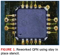
Numerous methods are used to rework leadless devices, either guided by the older IPC-7711, Method 5.4.1 process guidelines or the newest stenciling techniques. The older of these methods includes solder paste printing the site location on the PCB, followed by placement and reflow of the device. The newer method includes the device pad “bumping,” followed by placement of the device with a rework system using paste flux (Figure 1).
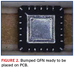
Several years ago, a simpler, faster method for reworking leadless devices was developed using polyimide stencils. In this method, a polyimide stencil is placed over the land patterns on the bottom of the device. Solder paste is then rolled into the apertures. After reflow, the stencil is peeled off, leaving “bumps” on the bottom of the device (Figure 2). A stencil permanently affixed to the PCB filled with paste flux or solder paste then acts as the receptacle for these device “bumps” to fit in to. However, heretofore the longevity of such an interconnection was questioned. This study, a portion of which is described in this writing, verifies the reliability of these solder joints using this newer technique.
Method
The goal of the NASA/DoD project was to generate data supporting qualification of SnPb rework procedures for military hardware built with Pb-free processes through analysis of thermal cycling, vibration and drop test data, including micro-section analysis.
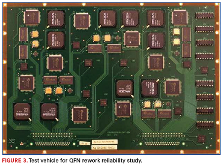
Thirty of the 193 test vehicles were built for Crane, in support of the larger Naval Supply Command (NAVSUP)-sponsored Logistics Impact of Pb-free Circuits/Components project. PCBs were assembled using SAC 305 Pb-free solder alloys using boards with Pb-free component finishes. The boards had an FR-4 laminate per IPC-4101/26 with a minimum glass transition (Tg) of 170ºC for the test vehicles. Bare boards complied with IPC-6012, Qualification and Performance Specification for Rigid Printed Boards, Class 3, Type 3 specifications. The boards had an immersion silver finish and were processed per IPC-4553, Specification for Immersion Silver Plating for Printed Boards. The test vehicle was 14.5"x 9" x 0.09" with six 0.5-oz. copper layers (Figure 3).
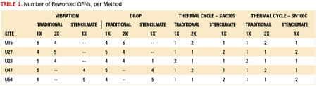
Following assembly, rework was performed on random Pb-free DIP, TQFP-144, TSOP-50, MLF, LCC and the QFN components of interest using SnPb solder. Components were reworked either once or twice. QFNs were reworked using two methods. In the first method, boards were PCB device locations paste-printed on the boards using rework systems. Devices were removed per IPC-7711, Method 3.11. In the second method, parts were bumped IPC-7711, method 5.8.1.2. Once bumped, the parts were inserted into the stencil on the board. The matrix of the experiment is in Table 1.
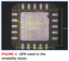
The particular focus of this paper is related to the QFN package (A-MLF20-5mm-.65mm-DC) as seen in Figure 4. The test plan was chosen to represent performance requirements in applicable military and industry standards. A key factor was selecting test parameters that would subject enough environmental stress to cause solder joints to fail, thus permitting differentiation between lead vs. Pb-free performance. MIL-STD-810F, IPC-SM-785 and IPC-TM-650 were primary references used for writing the test plan.
Numerous tests were part of the overall test protocol. The vibration test was instituted per MIL-STD-810F, Method 514.5 (Vibration), to determine reliability of the various solder alloys under severe vibration. Thermal cycle testing used was performed in accordance with IPC-SM-785, Guidelines for Accelerated Reliability Testing of Surface Mount Solder Attachments, to determine the longevity of the solder joints under thermal stress conditions. It was conducted at two different conditions: -55° to +125°C and -20° to +80°C. Thermal cycle tests were run until greater than 63% of component failures were achieved in order to provide statistically meaningful data. The mechanical shock test was used to determine solder resistance to the stresses associated with high-intensity shocks induced by rough handling, transportation, or field operation. The Combined Environments Test (CET) was used to predict reliability of solders under combined thermal cycle and vibration. Finally, drop testing was used to determine resistance of board-level interconnects to board strain induced by dynamic bending. These failure modes replicate the stresses seen during manufacturing, electrical testing (especially in-circuit test), card and field installation due to process issues and/or the quality of incoming components and/or boards.
Results
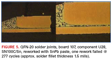
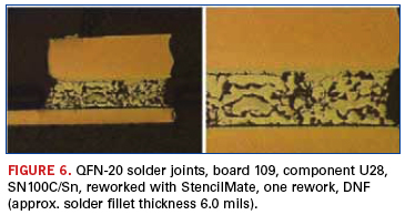
The polyimide stencil reworked solder joints were significantly thicker than the traditionally reworked solder joints (Figures 5 and 6).
Thermal cycle testing. Thermal cycling testing was conducted between -55° and 125°C per http://teerm.nasa/gov for NASA-DOD Lead-Free Electronics. The temperature was cycled between -55° and 125°C at a maximum rate of 10°C/min and a dwell time of 30 min. at 125°C and 10 min at -55°C. A total of 4,068 cycles were completed. Electrical continuity was continuously tested, and failure was recorded corresponding to the total number of cycles.
Vibration. Vibration testing was conducted per the study’s test protocol (available at teerm.nasa.gov). Test vehicles were evaluated at eight intensity levels from 8 to 28G. Each intensity level was evaluated consecutively, starting with 8G and increasing in intensity every 60 min. Table 3 outlines the vibration profile for each level as programmed for the shaker table. For all levels, the power spectral density (PSD) increased at the rate of 6db/octave between 20 and 50Hz and decreased at the rate of 6dB/octave between 1000 and 2000Hz.
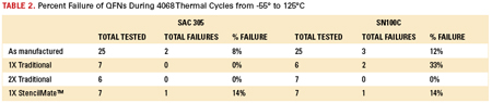
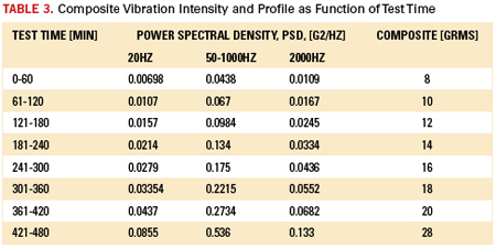
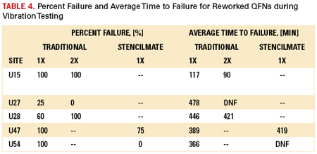
Table 4 shows results from the comparison of percent failure and time to failure for reworked QFNs. Percent failure was calculated by dividing the number of components in a group that failed during testing by the total number of components in that group. Average time to failure was calculated considering components that did and did not fail during testing. Differences in time to failure are considered significant if the percent failure differs by at least 40%. Drop shock, as well as other reliability test results, can be found on the teerm.nasa.gov website.
Conclusion
Based on the extensive reliability testing undertaken in this study, it was determined that independent of the QFN rework method, the polyimide stay-in-place stencil technique performed at the same level as traditional board paste printing. Based on thermal shock and vibration testing (as well as shock, combined environmental and drop testing), there was no difference between rework methods. These results have shown that this simple-to-implement technique has been shown to not impact the reliability of a reworked device. In fact, the microsections indicate that the stay-in-place polymide stencil technique, if time allowed, would outlast traditional hot air rework methods.
Bob Wetterman is president of BEST Inc. (solder.net); bwet@solder.net.
References
1. IPC-7711/IPC-7721B, Rework of Electronic Assemblies, 2008.
2. J.P. Tucker, C.A. Handwerker, A.E. Pedigo, et al, “NASA-DoD Pb-Free Electronics Rework Project: Effect of 1x and 2x Eutectic Solder Rework on Vibration Reliability,” SMTA International Proceedings, October 2011.
3. National Aeronautics and Space Administration, “NASA-DoD Lead-Free Electronics Project,” March 2010.
4. NASA-DoD Lead-Free Electronics Project Joint Test Report - Final, “Technology Evaluation for Environmental Risk,” December 2011.
5. National Aeronautics and Space Administration, “NASA-DoD Lead-Free Electronics Project,” September 2009.
6. Daniel Staubach, “QFN Rework in OEM Quality,” EMT Worldwide, March 18, 2008.


Press Releases
- Javad EMS Upgrades Through-Hole Soldering Capacity with New SEHO PowerWave System
- Sharpen Your Selective Soldering Skills with Kurtz Ersa's July VERSAFLOW 4/55 Training
- Omron Advances Inspection Technology with NVIDIA Omniverse and Metropolis
- Seika Machinery’s SMI 2026 Webinar Series Continues with Focus on PCB Cleaning Before Solder Paste Printing