

Nano-Coatings for Stencils
Lab tests reveal decreased print variation and question whether smoother surfaces show better paste release.
Nanotechnology is used to create new structures and components size 100 nm or smaller. A nanometer is one millionth of a millimeter. That’s approximately one fifty-thousandth the diameter of a hair.
This author invested considerable time researching limitations of the field of stencil fabrication and looked at crossover technologies that could be introduced into this specialty industry. Reviewing several potential candidates, nanotechnology1 rose above all others.
Typical coatings mechanically adhere to the surface of the target material to which they are applied. These types of adhesions usually are weak, which limits their effective life through delamination, etc. This leaves them susceptible to wear and tear that, after being exposed to mechanical types of cleaning, cleaning agents and even stress-inducing flexing of the foil, will cause them to flake. This in turn could contaminate the assembly.
Some nanotechnology coatings do fall into this category. From the author’s experience, the adhesion process of the coating is vital to a successful nanotechnology product for the stencil printing industry. Concerns include whether the coating has deviations within it, such as thickness variations due to pooling, or requires several coatings to be built up for durability. This could lead to inconsistent stencils.
Regardless of coating method, longevity and repellent characteristics, how may this new technology help the masses? Given that area aspect ratio is a performance driver, coating the bottom side of the stencil (substrate contact side) will affect a different factor of performance. With less adhesion of solder paste on the bottom side, cleaning and process maintenance may be easier.
There have been suggestions of users improving understencil cleaning process by significant factors with the introduction of nano-coated stencils.2 Based on lab tests, not only does this author concur, but observed a few other phenomena worth mentioning.
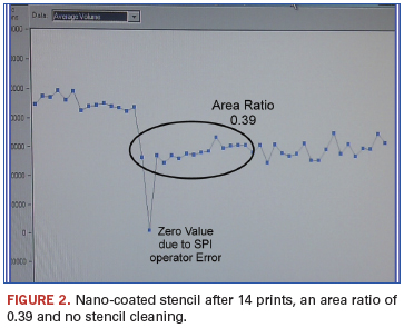
Stencil priming. The typical first few prints seem to prime the stencil apertures in typical stainless steel stencils (Figure 1). In most SMT assembly lines, it is not uncommon for the first two to four prints to show variation. This was not witnessed while printing with a nano-coated stencil. The first print was the same as the last, as shown in the real-time 3D volumetric data plots (Figure 2).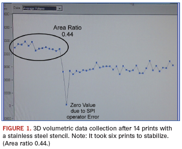
Paste wait time response. Printing was stopped and 30 min. allowed to elapse before printing was continued. Without any stencil cleaning, the first print showed no signs of deviation. And although there were symptoms of more variation than previously, it still was within a tolerable range for consistent assembly process control (Figure 3).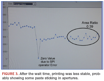
Stencil separation speed. Changing the speed of this parameter from 1 mm/s to no stencil separation speed control (maximum speed) revealed no noticeable change in the paste volume, other than an increase of overall mean volume (Figure 4). It is hypothesized that with less surface energy within the apertures, the print medium separates more efficiently due to a quick shearing effect, akin to pulling a soft stringy cheese and sharply snapping it to break it. 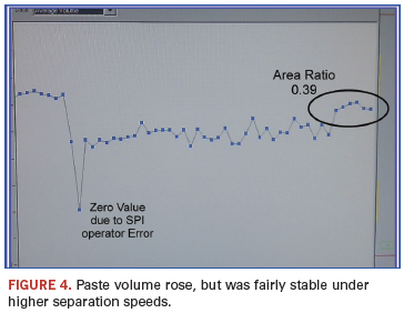
Conversely, a slow separation of the solder paste appears to create a kind of laminar flow, whereby the flux vehicle will separate from itself more easily than at the surface of the aperture wall. More investigation in understanding this phenomenon will be useful in identifying the physics underlying the surface tensions created by the print medium and area ratios. However, the focus here is on altering the surface energy characteristics to permit better release of material.
Nano Coating Integrity
Although a nano-coated stencil may show promise, how do you know it is coated? How do you know it is durable? New terminology will be introduced, such as hydrophobic/oleophobic, these being water and oil repellent, respectively. As water is not a printing medium used, more viscous materials such as flux in solder paste (fluxophobic) will need to be tested and verified. A number of tests can be applied, one being the contact angle test using a goniometer. Such metrology usually isn’t readily available, so taking a low angle lateral digital photograph and performing measurements using a PC works too.
For solder paste printing, flux would be an ideal medium to use for this. By applying a droplet of the flux material, the angle of contact reveals the nature of the surface energy (Figure 5). This test can be repeated for durability so that wear characteristics and, therefore, effectiveness can be ascertained after many print cycles, understencil cleaning cycles and stencil washes have been imposed on the stencil.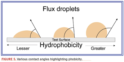
An easier practical test carried out on different materials consisted of a droplet/bead test and a run test. These test samples were cleaned and treated with a simple wipe on nano coating chemistry that has a self limiting nano layer. As the specific fluxes were not available at the time, a light oil similar in viscosity to flux was substituted. This is a comparative test, and the concept was to see how treated and untreated stencil materials behaved with respect repellency. Hydrophobicity is not a relevant test for performance.
Stainless steel SRA (stressed relieved annealed). This material is a little more ductile than other stainless steels and is used throughout the stencil industry for most standard products. The drop/bead and run test (Figure 6) clearly displays the difference in the level of oil repellency between nano-treated and untreated. One phenomenon observed was how the untreated run test would not leave the base material, whereas the treated material would run off to the paper below. Both treated and untreated samples are in contact with the paper. This was consistent with all tests with the different stencil materials used. This could be an interesting discovery of how surface tensions may also factor in paste release, with not just the aperture walls but the rims of the upper and lower surfaces playing a role. This would reinforce the idea that underside stencil cleaning paper will absorb and remove contamination more efficiently on a nano-treated stencil compared to an untreated stencil.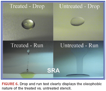
Stainless steel fine grain (FG). There is an increasing interest in the development of fine grained materials because this could be a solution for providing higher mechanical strength alloys.3 With finer grain structure, it is proposed that the newer laser cutting process will provide a smoother wall and thereby better paste release. The bead and run test (Figure 7) confirms that an untreated “smooth” surface does not repel the oil and, therefore, questions the theory that smoothness releases better.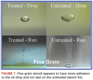
Nickel. Nickel has been supplied in various forms, from electroless nickel plating to the actual electroforming process. Nickel has an excellent natural lubricity and has had various technical publications promoting its superior paste release characteristics. The drop and bead test using the oil revealed characteristics far from the level of repellency required for good paste release, however (Figure 8).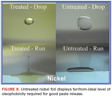
Nano-coated stencils may offer a wider process window and aid process maintenance. All of this can lead to higher throughput, higher first pass yield and aid with sensitive processes.4 It would be wise to review the longevity of such coatings, as there will be a cost involved, and if the coating life is only measured in a few thousand cycles, then the total value will need to be reviewed.
To summarize the key points regarding nano-coated stencils:
- Phobicity: Does the technology exhibit the flux/oil repellency required for successful process control?
- Durability: Long “economical” usable life that fits the assembly environment.
- Lead time: Does the technology fit within the quick turnaround demand?
- Cost: Compare price to performance and process needs.
- Coating technology: How is it applied and can it be re-applied if minor damage has occurred?
- From an in-depth exposure to this technology, it became clear that various coating methodologies are utilized. However, the underlying technology shows promise to bring the stencil capability to the next level of process performance.
References
1. Alan Rae, “Nanotechnology Is Now Starting to Find Applications in Electronics,” SMTA Pan Pacific Symposium, January 2010.
2. Carmina Läntzsc, “Nano-Coated SMT Stencil with Anti-Adhesion Effect: A Novelty in Electronic Production,” EPP, September 2008.
3. Stephanie Brochet, “Mechanical Behaviour of Ultra-Fine Grained Austenitic Stainless Steel, Fracture of,” Nano and Engineering Materials and Structures, 2006.
4. Miguel A. Lara, “Laser-cut Electropolish and Laser-cut Nanocoat Stencils: A Comparison of Finish Performance for Complex Designs,” SMT, April 2010.
Ricky Bennett is president and CEO of Assembly Process Technologies (assemblyprocesstechnologies.com); rickybennett@assemblyprocesstechnologies.com.


Press Releases
- XLR8 EMS Welcomes Raul Jorge Lopez Jr. as Director of Program Management and Procurement
- Koh Young America Promotes Ramiro Mora to Lead Service and Applications in Mexico and South America
- ViTrox Americas Welcomes Huy Pham as Technical Support Engineer
- XLR8 EMS Appoints Steve Dutton as Chief Sales Officer