

Fundamentals and Benefits of Vapor Phase Reflow Soldering
Do the smaller machine footprint and thermal advantages offset increased voiding?
EMS providers build many types of PCB assemblies, and as a result, must have available whatever technologies might be necessary to process a particular assembly. Like the slogan from the pawn shop television series, “You never know what’s going to come through that door.”
For SMT solder reflow, we offer two types: forced convection reflow and vapor phase reflow. Why? For some types of assemblies, vapor phase does a better job. It’s fast; no inert atmosphere is required, and there is no possibility of overheating the assembly. There are downsides too, and the appropriate reflow technology is based on each particular assembly. Let’s look at both vapor phase condensation heating and forced convection reflow. The two actually grew up together.
VPS has been around at least as long as conveyorized infrared (and later forced convection) reflow soldering, perhaps even longer. The first patent describing vapor phase reflow soldering dates to 1973. Vapor phase began as a batch process, primarily with hybrid microelectronics, compact circuits on small-area alumina substrates, and initially demonstrated a number of key qualities and advantages, including a rapid and uniform rise to reflow temperature and quality solder joints. The rapid (almost instantaneous) rise to reflow temperature, the rate of which could not be controlled, proved to be a liability later when SMT PCBs became larger in area, with multiple layers, epoxy-glass laminate construction, and other evolving characteristics. For a time, a rivalry ensued in the SMT PCB industry between proponents of vapor phase and those promoting IR reflow, which permitted creation of oven temperature profiles that could control the rate of temperature rise in the PCB in-process.
Early vapor phase systems were relatively simple. A reservoir of inert, clear perfluorinated liquid was heated to its boiling point, which happened to be slightly above the solder liquidus temperature. Several different formulations of the liquid were available, in a narrow range of temperature boiling points matched to various common eutectic popular solder alloys available at the time, such as Sn63. When the liquid boiled, it created a vapor blanket above the reservoir of liquid. When a PCB was lowered into the vapor, the vapor condensed on the PCB, bringing it rapidly up to the temperature of the boiling liquid, causing the solder connections (typically printed or dispensed solder paste) to reflow and form solder joints. After a brief dwell in the vapor to permit proper wetting and solder joint meniscus formation, mere seconds, the PCB assembly was hoisted back out and permitted to cool, the excess liquid draining off the PCB and back into the boiling sump (FIGURE 1). There was very little liquid loss, since the interior of the process chamber above the vapor blanket layer was ringed with cooling coils that constantly condensed any vapor that rose above the vapor blanket. (Liquid trapped under components, for example, and thus lost that way was termed drag-out.)
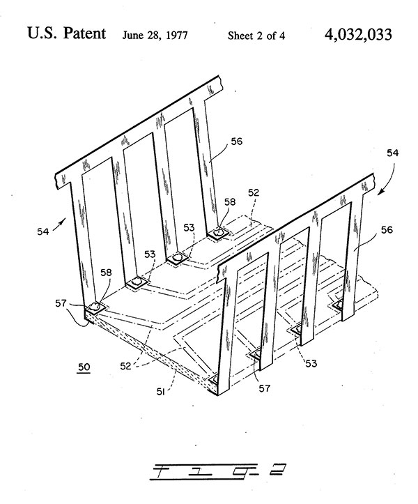
Figure 1. A diagrammatic representation of a partial sectional view, in elevation, of a condensation heat transfer facility, as described in a 1977 Lucent patent.
The perfluorinated liquids used in the vapor phase process were (and are) inert, even non-toxic. In the early days, salesmen for vapor phase technology would sometimes drink a small amount in a paper cup, when making an impassioned pitch, to show how harmless it was, reportedly without ill effects.
Also, the reflow environment of the smothering vapor blanket discouraged and even prevented oxidation, resulting in good wetting, shiny solder joints, and in most cases precluded the need to clean the PCB afterward. The primary problem with vapor phase was its uncontrollable rate of temperature rise in the part or in the assembly being soldered. This rapid rise became a problem, as PCBs became more complex in the variety of materials from which they were manufactured and expanded to multiple copper layers. Thermal coefficient of expansion (TCE) of components and boards with alternating layers of copper and epoxy-glass (having different TCEs) became a concern. The consensus emerged that the temperature of SMT PCB assemblies should rise a maximum 2°C/sec. Otherwise thermal stress could damage the board. This, of course, created a problem for vapor phase processing, since there was no way to control ramp rate. Different techniques were tried to lessen the impact of the rapid ramp to reflow, including preheating the assembly prior to immersion in the vapor. The inability to control this thermal ramp eventually led to forced convection reflow winning the day, because having multiple heating zones allowed the process engineer to sculpt a thermal profile for a board, raising the temperature to reflow in stages at a controlled ramp, permitting the various materials in a PCB (e.g., copper layers, epoxy-glass laminate, and components with widely varying tolerances to variations in TCE or delta T) to equilibrate in temperature, minimizing the potentially damaging effects of thermal stress. This concept of multi-zone control became critical with the advent of large backplanes and other heavy, multilayer, large-dimensional PCBs.
Well before the development of forced convection, in the beginning of the vapor phase-IR reflow rivalry, IR processing was at a disadvantage because panel or “area source” IR was not yet developed, and IR sources were lamps or quartz rod emitters. These produced what was referred to as short-wavelength IR, which could be color-selective and would therefore not heat PCBs and components uniformly. Dark-colored components would wind up hotter than light-colored ones. These systems were also sensitive to conveyor belt loading. Too many PCBs spaced too closely together resulted in cold solder joints. These problems were gradually solved by the development of forced convection reflow systems. But initially there was a good argument for vapor phase: FR-4 SMT PCBs did not char or burn in a vapor phase system, since peak temperature could not exceed the boiling temperature of the liquid.
The operation of a vapor phase system is also fundamentally different from that of a linear conveyorized convection oven. PCBs are reflowed using the vapor “phase” of the boiling inert heat transfer liquid, and overall the footprint of a vapor phase processing system is smaller than that of a reflow oven, since, after all, the PCB assembly moves vertically up and down instead of horizontally across a series of heat zones on a moving conveyor.
The vapor layer transfers heat to the PCB and associated components as the assembly is enveloped by it. The heat transfer rate is high; the process is characterized by good wetting, and the process itself requires much less power input. The vapor phase process produces very little temperature difference between components of different thermal mass on the PCB. This makes the process very suitable for densely populated PCBs.
In a vapor phase oven, limitations of the physical temperature reliably prevent overheating of any part in the soldering process. As the vapor has a higher density, it is heavier than the surrounding air. This permits soldered parts to remain sealed inside an inert vapor atmosphere. Expensive nitrogen blanketing isn’t required to prevent oxidation and promote wetting. Also, the thermal processing area is naturally contained; for example, the inert fluid boils at 230°C and creates the vapor layer above it at 230°C. The air over the vapor blanket, however, does not heat up more than 50° to 80°C.
The heat transfer fluids such as perfluropolyether used in modern vapor phase reflow ovens do not contain CFCs or other harmful ingredients that could limit transport and storage of these liquids. Its main properties are excellent chemical and thermal resistance, very high electric insulation properties, non-toxicity, low viscosity, and no flash or fire point.
Convection Reflow Ovens
With multiple heating zones, sometimes as many as 12, followed by a cooling element, convection reflow ovens typically have individual temperature controls for each zone. After the SMT assembly process is completed, a conveyor belt carries the populated PCB into the oven, which exposes the PCB to a controlled time-temperature profile.
PCB assembly lines usually locate the convection reflow oven in-line with the other SMT assembly equipment, permitting relatively high throughput, without additional handling. However, each product requires its own reflow profile, which the engineering team has to create before start of production.
Convection reflow ovens usually have a large footprint and, therefore, consume a large amount of floor space in the factory. Although each heating zone has its own temperature control, it is not possible to control the temperature for an individual component.
Controlling Vapor Phase Heat Transfer
Heat adjustment. Engineers adjusted the temperature gradients in earlier vapor phase machines by regulating power to the heating elements. The greater the power transferred to the heaters, the more vapor was produced, and thus more heat could be transferred to the PCB assembly, even though this did not change the boiling point of the liquid.
As mentioned, the soldering process takes place in an oxygen-free vapor atmosphere, which minimizes the potential for oxide formation and improves wetting. However, the slight time delay in the creation and subsistence of vapors with the heater controls prevents the creation of sophisticated temperature profiles. Searching for a solution has led to the development of soft vapor phase (SVP) machines.
Level adjustment. The benefit of the SVP process is the immediate temperature gradient can be controlled as a function of the height of the PCBs above the surface of the liquid. In the SVP process, as the PCB moves deeper into the vapor blanket, its temperature rises. Holding the board at a certain depth achieves preheating of the board. As the depth increases, the board reaches liquidus temperature. By preselecting and controlling the soldering time automatically, engineers may create nearly any thermal profile necessary. Once soldered, the process moves the board up to the vapor boundary to lower temperatures and finally lifts it out of the vapor to cool down. The SVP process does not require additional mechanisms to control overheating, since, as mentioned before, the peak temperature of the PCB is limited to the boiling point of the liquid.
With VPS, void formation is unavoidable. Voids diminish or compromise the electrical and thermal conductivity of the solder joint. To mitigate voids, engineers prefer a vacuum-controlled process that facilitates outgassing them. Reducing the pressure over the liquid lowers the boiling point of the liquid; increasing pressure has an obverse effect. Use of vacuum extends the time above liquidus by about 30 sec., and this effectively reduces the number of existing voids and prevents formation of new ones. Void reduction must be conducted when the solder joints are liquidous, of course.
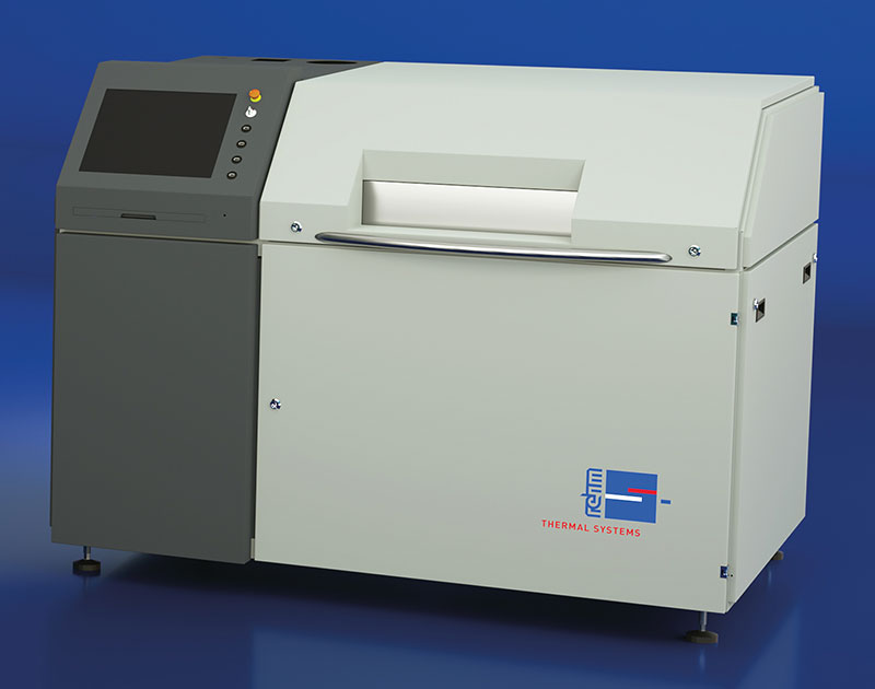
Figure 2. A modern vapor phase reflow system. Today, the soldering procedure can be individually regulated, and may include a vacuum module for void-free soldering.
Conclusion
The vapor phase soldering process transfers heat at about 100 to 400W/m2 K, considerably higher than 10 to 60W/m2 K of heat transferred by convection reflow soldering. Moreover, heat transferred by vapor phase is uniform for all components of the PCB, reducing the potential for thermal stress during soldering, provided the thermal ramp rate is controlled. The ability to optimize the thermal profile with extended peak times makes the process suitable for most types of electronics. The vacuum-controlled process facilitates outgassing of voids, leading to uniform, reliable joints.
Register now for PCB West, the largest trade show for the printed circuit and electronics industry in the Silicon Valley! Coming Sept. 11-13 to the Santa Clara Convention Center.


Press Releases
- Seika Machinery to Host SMI 2026 Webinar Series Session 2 on PCB Slicing Methods and Low-Stress Separation
- Pillarhouse USA Expands BarTron, Inc. Sales Territory into Indiana
- Mycronic appoints Peter Andries as General Manager of MRSI Systems and VP of Global Technologies Division
- The Test Connection, Inc. Becomes First Test Engineering Company in Space