

Solder Paste Qualification Testing for EMS Production
A consolidated test plan that gauges key solder paste properties and requires less than one shift of line time per product evaluated.
When a small EMS provider determined it was time to update its SMT process chemistry, it needed a test program it could execute efficiently, while keeping production running and costs under control. A review of existing SMT practices revealed an opportunity to improve quality and throughput by updating the solder paste chemistry used on the assembly lines. The incumbent did not exhibit best-in-class performance in printing or wetting. The subpar print and reflow performance was impacting quality and throughput, creating bottlenecks at print/SPI, at AOI and at rework areas.
A quick substitution of another paste formulation from the same manufacturer demonstrated an instant print quality improvement, enough to justify the time and expense of a solder paste qualification.
Solder pastes have over 20 properties or tendencies that can influence SMT assembly quality. Appendix A (online) lists them, along with their impact on the SMT process, how to test for them and the associated test criteria.
It is unrealistic to test individual paste properties in serial format; for efficiency purposes they must be nested in a designed test.
Furthermore, it is unrealistic to expect top performance in every category. Tradeoffs are always made in solder paste formulations; an ingredient that helps one tendency can harm another. The current solder paste is an excellent example. It has very good post-reflow properties, such as pin testability and corrosion resistance, at the expense of in-process properties such as print and reflow.
It is critical to understand the compromises and how they affect the process and end-product in order to make a well-informed decision on process chemistry. To that end, four candidate solder pastes were tested as identically as possible – on the same assembly line, with the same lot of PCBs, using the same stencil, run by the same operators/engineer, and all judged by the same criteria. All four solder paste candidates were among the industry’s current top-performing SAC 305 no-clean products.
Test Methods
Test vehicle. The original plan used a new test vehicle designed for evaluating solder pastes in miniaturized applications.1 FIGURE 1 shows Side A (the “top side” or “populated side”). FIGURE 2 shows Side B (the “bottom side,” “reflow side” or “unpopulated side”).
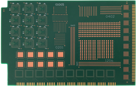
Figure 1. Side A of test vehicle.
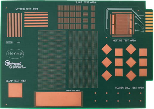
Figure 2. Side B of test vehicle.
The test board, at its beta stage of design during this evaluation, incorporates print and component-based tests for components as small as 01005s and 0.3mm WLPs on the populated side. The unpopulated side contains test patterns for wetting, spread, slump, solder ball/coalescence, cleanability/SIR and an extensive array of fine features referred to as Print-To-Fail (PTF) test pattern.
Upon receipt at the testing facility, some deficiencies were noted on the PCB fabrications. Many of the smaller pads were over-etched – some to the point of disappearance – and the stretch in the board made alignment of the stencil apertures and pads extremely difficult. Although all solder pastes would be evaluated under the same conditions, the PCB would not give an accurate indication of paste performance, especially the critical Print-To-Fail (PTF) patterns on which so many print tests are based.
To capture the critical PTF data, an off-the-shelf test vehicle2 containing similar patterns was substituted for Side B of the planned test board. FIGURE 3 shows the board. It is a popular industry test board and is stocked by a dummy component supplier.
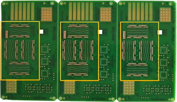
Figure 3. Substitute test vehicle with PTF patterns outlined.
Assembly equipment. The assembly line was configured as follows:
- Print: MPM Momentum HiE.
- SPI: Koh Young 8030.
- Place: Panasonic NPM-W.
- Reflow: Vitronics 820 XPM3 oven.
- AOI: Koh Young Zenith AOI.
All equipment is relatively new, well maintained and in excellent condition.
Test sequence. Because two different PCBs were used for print and reflow analysis, the original test plan was adapted to accommodate the different boards.
Part 1: Developmental board for reflow tests
- Paste was kneaded per technical support directions.
- Three new PCBs were printed.
- All PCBs were processed through SPI.
- The first PCB was unpopulated and reflowed without components to look for signs of spattering, wetting, spread or fusion issues.
- The second PCB was populated and reflowed immediately to simulate a typical production run.
- The third PCB was populated, held for four hours at ambient environmental conditions, and then reflowed to check for propensity to solder ball through moisture absorption and other environmental sensitivities similar to those listed for PCB 1.
- Both populated PCBs were processed through AOI.
- The five MLFs on each PCB were x-rayed for voiding analysis.
Part 2: Substitute board for print tests
- Paste was kneaded per technical support directions.
- Stencil under-side was cleaned with extended cycle to ensure cleanliness.
- Nine new PCBs were printed.
- Standard solvent-vacuum-vacuum wipe applied.
- Tenth board was printed.
- Eleventh board used for cold slump.
- Twelfth board used for hot slump.
- Approximately 20 more (previously printed and cleaned PCBs) were printed to work the paste before the abandon test.
- Four-hour abandon.
- Standard solvent-vacuum-vacuum wipe3,4 applied.
- Print boards 101, 102 … 110 to gauge response to abandon and number of prints to get the paste back to good working range of viscosity.
For the multiple categories tested, a score card was developed, and each category was weighted in accordance with its importance to the operation and performance expectations of the process engineers.
Results
Solder paste printability analysis. There are two simple statistical methods for quantifying print transfer rates and their consistency. Using a solder paste inspection (SPI) system that employs moiré interferometry, each individual deposit is measured, and its volume, height and area (among other data) are recorded.
Both analysis methods use the same basic statistics – the average and standard deviation – to describe the quality of the solder paste prints. One method normalizes the spread of the data, or standard deviation, by expressing it as a percentage of the average. This is known as the coefficient of variation (CV), and is often indicated as an annotation or color-coded data point when the average solder paste transfer rates are plotted. As a general rule, 80% transfer efficiency (TE) with less than 10% CV is desired. Up to 15% CV may be acceptable on challenging prints, but greater than 15% indicates an out-of-control process and is considered unacceptable.
The second metric uses the same averages and standard deviations as the first, but includes target values and specification limits in the calculations to form a composite index of process capability known as Cpk. Because the index is affected by both the spread of the data and its proximity to the target value, any drift in average TE, either above or below 100%, will negatively affect the Cpk value. Values of 2.0 or higher are desired, as 2.0 indicates a very robust 6σ process. Cpk values of 1.67 or more are often considered acceptable (5σ+), as many processes inherently struggle to meet the 2.0 mark.
In this print test analysis, TE and CV are used first as a baseline check to compare with similar data to ensure good system performance, and to determine the edge of the process window where paste performance is well-differentiated among the candidates. Cpk data are then used to characterize each paste’s capability relative to each other in terms of fine feature print capability, and examine the print data board-by-board.
Print data from the PTF patterns was analyzed using the typical approach for this test PCB design:
- The best case print scenario is square, solder mask-defined pads using square stencil apertures
- The worst case print scenario is round, copper-defined pads using round stencil apertures
- Note the two cases in between best and worst, i.e., square copper-defined and round mask-defined, have historically fallen between on this test vehicle and are no longer typically analyzed because they offer less insight into print behavior.
Solder mask-defined (SMD) pads provide better gasketing against the stencil than copper-defined (or NSMD) mask) pads and therefore better, more repeatable print quality. Square apertures transfer solder paste better than circular ones because of the unequal adhesion forces along walls and in corners. Therefore, out of the four test combinations of circle/square and SMD/NSMD, the two that are typically reviewed first are the best and worst cases, or square/mask-defined and circle/copper-defined.
The first 10 prints, on new, unused PCBs, were analyzed. Results are shown in FIGURES 4 and 5, where the different solder pastes are represented by different line colors, and the CV is indicated by the color of the data point. Again, the typical benchmark to indicate a controlled process is a minimum of 80% transfer and less than 10% CV (green). Up to 15% CV may be acceptable depending on the feature (yellow), but over 15% is unacceptable (red). The sample size for each data point shown is 480.
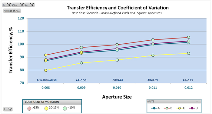
Figure 4. Transfer efficiency and variation on PTF patterns using best-case scenario.
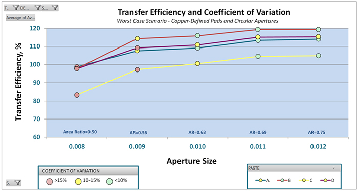
Figure 5. Transfer efficiency and variation on PTF patterns using worst-case scenario.
In the best case scenario (Figure 4), Paste B showed the best transfer and acceptable variation down to the 0.56 area ratio. Paste C showed the lowest transfer, although still better than the 80% benchmark, and acceptable variation down to the 0.56 area ratio (AR). Pastes A and D printed similarly to each other, transferring less paste than B but more than C; however, unlike B and C, their variation was unacceptable at the 0.56 AR. Each paste maintained its rank in transfer efficiency throughout the range or ARs.
In the worst-case print scenario of circular, copper-defined pads (Figure 5), Paste B again demonstrated the best transfer and held acceptable variation down to the 0.56 AR. Also again, Paste C showed the lowest transfer, and its CV rose above 10% at the 0.63 AR. Again, maintaining their ranks, pastes A and D demonstrated TEs in between pastes B and D, but while paste A’s variation remained good, D’s was unacceptable up to an AR of 0.56 and marginal throughout the rest of the ARs.
Paste D appeared to show good release, but completely unacceptable variation. Further investigation showed the source of variation was two boards, prints #4 and 6, which got little or no solder paste. The engineer running the tests indicated the solder paste was sticking to the squeegee blades, and videoed it curtaining off the blades incorrectly. The data were then analyzed for a 10-print sequence starting with print #7 to see if it stabilized, but it showed more problems on prints #9, 11 and 13. This product did not demonstrate print performance representative of the class of materials in which it is considered. Somehow, it may have been compromised somewhere in the supply chain.
This test vehicle has been used extensively, and with the exception of Paste D, data collected during the 4Front trials are similar to that collected using other solder pastes, printers, and SPI systems. Typically, the mask-defined squares should print well down to the 9 mil in a 4mil foil or an AR of 0.56. Because there is greater challenge in the round, copper-defined pads, they typically begin experiencing print issues in the 10 mil aperture size, or 0.63 AR range. As a basic reality check,
these data track with the findings of many other studies, with the exception of paste D.
This first cut of data indicates the edge of the process window, or the best area for further investigation to differentiate print performance. It is indicated by the yellow data points in the TE graphs. For the best-case scenario of mask-defined squares, that’s 8 mil (AR=0.50) features. For the worst-case scenario of copper-defined circles, that’s in the 9 to 10 mils (AR=0.56-0.63) range.
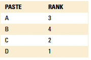
Cpk to gauge process capability with higher resolution. To gain insight on fine-feature printability, Cpks were calculated for each feature size and shape in the PTF patterns and a database constructed to query them. The process capability indices are then used to explore the lower edges of the process window as indicated by the TE/CV analysis. FIGURES 6 to 10 show the Cpks on a print-by-print basis for the first 10 prints.
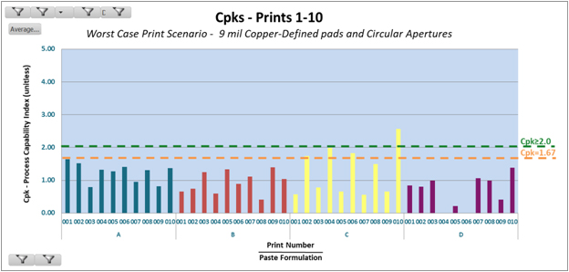
Figure 6. Cpks of worst-case features at lower edge of process window (AR=0.56).
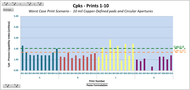
Figure 7. Cpks of worst-case features at lower edge of process window (AR=0.63).
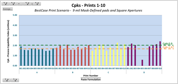
Figure 8. Cpks of same size features as Figure 6, except with best-case padstack (AR=0.56).
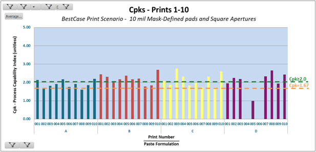
Figure 9. Cpks of best-case features at lower edge of process window (AR=0.63).

Figure 10. Cpks of best-case features at lower edge of process window (AR=0.50).
As described previously, the process capability index, or Cpk, indicates both the distribution of the data and its proximity to the target value and specification limits. For the calculations in this report, target values of 100%, with upper and lower control limits of +/-50%, were used. These are the typical default specifications on SPI equipment. The sample size for each print is 48.
Cpk values of 2.0 or higher are desired, as they indicate a Six Sigma process. Six Sigma repeatability can be a difficult goal to meet; new processes are often developed to meet Cpk values of 1.67 or 1.5, depending on their degree of difficulty.
The Cpk values tell an interesting story. Paste D shows negative Cpks on prints 4 and 6. This occurs when the mean value falls outside a specification limit – in this case, the lower limit. Paste B has lower Cpks than either paste A or C, primarily because B released more than 100%, moving its average away from the 100% target. Paste A, which consistently had more variation than B (roughly 1 to 2%), had better Cpks because its mean volumes were closer to the target. The same applies to paste C, which had by far the lowest release, but was also closer to the target. Overall Cpks were much higher on the 10 mil (AR=0.63) than the 9 mil (AR=0.56).
Compare the values of the difficult-to-print padstack with the easier-to-print padstack. Figures 8 and 9 show the Cpks for the best case.
The 9 mil mask-defined square pads and apertures printed better and more consistently than the 9 or 10 mil metal-defined circular pads. The 9 mil feature size represents a 0.4mm BGA. A quick comparison of the responses between mask- and metal-defined pads provides DFM guidance for PCB layout. Finer features print far more robustly on mask-defined pads. Furthermore, a quick visual comparison of transfer efficiencies (Figures 4 and 5) shows mask-defined pads maintain TEs closer to 100%, whereas metal-defined pads often show more than 100% TE due to gasketing issues.
Figure 10 shows the true edge of the process window for mask-defined pads and square apertures. When the effects of metal-defined gasketing issues are resolved and deposits center more closely around 100%, paste B is clearly the most consistent. Paste A shows good capability also. In the more difficult-to-print feature types, Paste C shows a repetitive up-and-down trend similar to that of partial squeegee sticking. Paste D could not produce 10 decent prints in a row.
Observations
- Paste D had negative Cpks on boards 4 and 6 because their means fell below the lower specification limit of 50% aperture volume. The raw data showed a lot of null reads. This appears to be paste sticking to the squeegee after prints 3 and 5.
- Paste C also showed an interesting pattern of ups and downs with each squeegee stroke on the copper-defined 9 mil circles. This pattern could be interpreted as differences between front->back and back->front strokes. The pattern is not repeated on the other data sets, however, so it is more likely related to paste release off the squeegee. Paste C showed far more inconsistencies on the metal-defined pads.
- On the more challenging circular pad stacks, Paste A had higher Cpks than Paste B, but Paste B had higher release and similar variation. Because both released over the target value of 100%, the higher release is farther from the center of the process window and therefore has a lower Cpk.
- Paste B consistently released more than Paste A regardless of pad and aperture design, but statistically they were both equally consistent in the spread of the data.
From a transfer efficiency and repeatability perspective, Paste B is the best candidate and Paste D the worst. Of the two remaining candidates, Paste A releases better than C, but C is much more consistent. They are ranked in TABLE 1.
Table 1. Rank Order for Paste TE and Repeatability (the higher the better)
Tendency for peaking or stringing. The tendency for peaking or stringing can often be assessed by comparing the heights of rectangular deposits for QFNs. If two solder paste deposits have similar volumes but different heights, then it is easy to conclude the one with the higher average height has higher peaks on the ends. In this case, the height differences tracked with the volume differences in the same rank, so the tendency for peaking is more difficult to assess. The only conclusion that can be drawn is from pastes A and D, which deposited similar volumes. Paste D’s readings showed much higher peaks than paste A. Paste D continues to demonstrate substandard print capability.
Wipe sensitivity. Because a wet-vac-vac stencil under wipe was run between boards 9 and 10, a jump in Cpks between boards 9 and 10 indicates a wipe sensitivity. Pastes A, C and D all showed capability jumps after the wipe for both borderline feature sizes, as seen in figures 11 and 12. Paste B did not appear to need that wipe after board 9. The rankings are shown in Table 2.
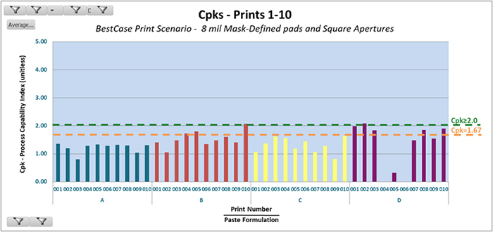
Figure 11. Cpks before and after wipe (9 and 10) and pause (10 and 101) for 9 mil metal-defined circles.
Figure 12. Cpks before and after wipe (9 and 10) and pause (10 and 101) for 10 mil metal-defined circles.
Table 2. Rank Order for Paste Wipe Sensitivity (the higher the better)
Wipe sensitivity is not as prominent in mask-defined padstacks, primarily due to the improved gasketing. Therefore, mask-defined padstacks were not analyzed for wipe sensitivity.
Abandon time. All pastes were subjected to a four-hour abandon time. After the abandon and prior to the first print afterward, they were solvent-vacuum-vacuum wiped. Comparing prints 10 with 101 indicates the solder pastes’ responses to the long printing pause. Comparing the number of prints to regain capability indicates the relative need for kneading prior to printing or after a pause.
- Paste A lost print capability after the pause, but recovered it in 2 prints.
- Paste B showed little, if any, print capability compromise after the pause.
- Paste C lost print capability but seemed to recover better than paste A.
- Paste D also lost print capability and was generally the poorest performer.
Final ranks are shown in TABLE 3.
Table 3. Rank Order for Paste Abandon Time (the higher the better)
Slump tests. Slump test patterns printed on the board were inspected visually and with SPI. The cold slump boards, which aged 20 min. at ambient, and the hot slump boards, which aged 20 min. at 185°C, showed no discernable differences in deposit quality, bridging, or increased areas. Slump tests performed onsite showed little differentiation and are considered inconclusive. This will not impact overall test results, as slump testing is part of solder paste development, and most modern lead-free pastes have little or no known issues associated with slump.
Reflow analysis. Standard reflow profiles were developed for each solder paste in conjunction with the supplier’s technical support engineer. The profile for each candidate solder paste can be seen in Appendix B.
QFN voiding. Five different ground pad designs were used in this test (FIGURE 13). Two assemblies were x-rayed for each solder paste type. During the initial phase of the investigation, the void calculation algorithm needed fine-tuning, so the x-ray images were captured without the calculations and visually compared and ranked. The images and their ranks are shown in Appendix C.
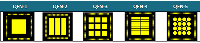
Figure 13. Different QFN ground pad solder paste patterns.
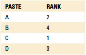
Visual assessment of void formation ranked the pastes from best to worst as A, B, C, D, with A being far better than B, and C and D performing similarly.
When the void calculation algorithm was ready, one set of assemblies for each paste were analyzed. The results, and their ranks, are shown in TABLE 4.
Table 4. Void percent, number of voids, and average void size for each QFN ground pad design and solder paste
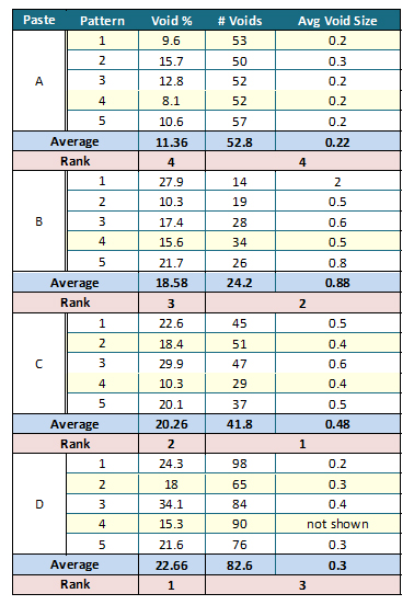
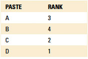
The numerical analysis of one board from each paste ranks the voiding performance (from best to worst) as Paste A, B, D and C, again with very little differentiation between C and D. These results concur with the visual analysis of the voiding behavior.
Table 4 also shows the lowest void-forming aperture designs, QFN-2 and QFN-4, by highlighting their results in yellow. The numerical analysis also concurs with the visual analysis for void-minimizing aperture design.
Coalescence or graping. Solder joints on 01005, 0201 and 0402 (imperial) components were photographed; representative images are shown in TABLE 5.
Table 5. Reflow Images
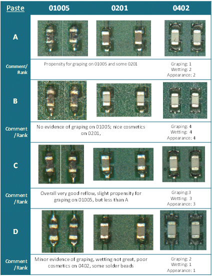
Solder paste A showed the strongest tendency to grape, or fail to completely fuse during the reflow process. Paste B showed little to no graping. Paste C showed excellent wetting but a small amount of graping. Paste D showed poor wetting and poor joint cosmetics, further indicating potential damage to the solder paste prior to the test. Referencing the scorecard in Appendix D, in order of overall reflow performance on small chip components, pastes rank in order from best to worst: Paste B, A, C and D.
At this juncture, solder paste D will be excluded from further analysis, as the remaining tests are more labor-intensive, and based on print, void and joint formation results, D is no longer considered a viable candidate for this operation. The extensive graping of paste A on 01005s is also considered a disqualifier.
01005 tests. The 01005 tests run in this experiment were a baseline test for this assembler. As the operation gears up for 01005 capabilities, qualified placement equipment was purchased, upgrades for SPI and AOI ordered, and investments were made in new-generation optical and digital microscopy tools.
On the solder paste trial run, the SPI and AOI upgrades had not been implemented. The SPI failed all the 01005 solder paste deposits for insufficients. The 7x8 mil apertures have area ratios of 0.47 in the 4 mil foil used, and the resulting small deposits barely crossed the 40µm threshold of the SPI machine, as viewed on its screen.
An alternate method of gauging the solder paste print is by viewing x-ray images of the solder joints after reflow. Larger deposits will create darker images, and smaller deposits will create lighter images. Examples of insufficients, opens and solder balls are shown in FIGURE 14, and the images from each solder paste are shown in FIGURE 15.
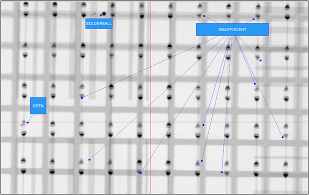
Figure 14. Types of 01005 defects visible in x-ray analysis.
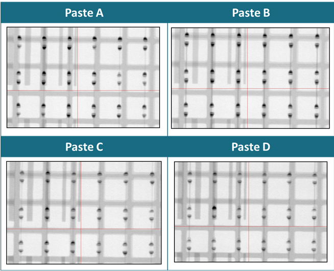
Figure 15. Results of 01005 x-ray for each solder paste.
Differences in 01005 performance were qualified relative to each other. Paste B had the most consistent deposit sizes and solder joints. Paste A had the most inconsistency.
Visual inspection. None of the unpopulated PCBs showed any signs of spattering or other reflow issues. The samples will be re-inspected using the new video microscopes.
Mid-chip solder balls (MCSB) on 0201s had historically been an issue for this operation. They were successfully addressed with aperture design changes. The test stencil used both the suggested aperture design and the assembler’s new design. No MCSBs were found on the 0201s for any of the solder pastes tested.
Side-mount LEDs floating and skewing were also a nagging issue with the incumbent solder paste, so they were mounted on 1206 pads. No floating or skewing was noted with any of the candidate solder pastes.
Several 0402s were skewed on one board. They were mounted in close proximity to each other and appear to be a handling issue. No defects were attributed to the solder paste, but the defects and likely root cause are noted for the record.
AOI programs found no missing, skewed, tombstoned, tilted or misplaced parts on the 0201 or larger components. Data for 01005s were collected as a baseline for comparison after the upgrades were installed.
Testability and residues. Initial visual examination of the residues by test engineering did not reveal any obvious problems. Originally, a flying probe test was planned to differentiate among the four candidates. However, after paste D was eliminated due to overall performance issues, and paste A was eliminated for reflow performance, a flying probe test was not deemed necessary. Data will be collected on paste B during its beta runs and compared with the incumbent products, and PM schedules may be varied based on the results.
Cleanability. Bottom-termination components and other packages with low standoffs are specified to run in no-clean-only processes, because their low clearance makes full dissolution and removal of the flux residues very challenging. Yet, CEMs are asked to do it every day. It is imperative the cleaning chemistry and process are compatible with whatever solder paste is selected.
The operation’s cleaning process was developed in conjunction with its chemistry supplier, and the correct levels of cleaning chemistry are automatically maintained in a closed-loop process. Upon discussions with the supplier regarding compatibility testing with the solder pastes, the operation was assured all four pastes had been tested with their current solvent system. The supplier provided reports on its internal tests with all four candidate solder pastes. The solvent will not need changing, but the concentration may require minor adjustment.
Scorecard. The solder paste scorecard (FIGURE 16) itemizes the major and subcategories on which solder pastes were rated, along with the criteria used to rate them. In each subcategory, the performance of each is ranked on a four-point scale, with 4 the best and 1 the worst. The subcategories are then totaled for an overall category score, which is then weighted based on importance to the operation. A larger, more legible image of the scorecard can be seen in Appendix D.
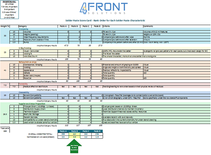
Figure 16. Customized solder paste scorecard.
Discussion and Conclusions
Review of the scorecard, and the strengths and weaknesses of each solder paste relative to each other, demonstrates the tradeoffs in solder paste selection.
- Paste B was the best at print and reflow, but not at voiding. It was not sensitive to wipe frequency or abandon time, giving it a very robust stencil life, excellent for low- to medium-volume manufacturing.
- Paste A was very good at print transfer and repeatability, great at voiding, but had problems at reflow, and showed poor recovery after abandon time.
- Paste C printed well in that it was very consistent and had the best repeatability. Its release properties weren’t as good as two other pastes, but voiding and reflow were respectable. Its two weak spots were under-wipe sensitivity and abandon time. Overall it is a good general purpose solder paste because, while it does not excel in any particular area, it has no fatal weaknesses either.
- Paste D appeared to be compromised from the beginning. It showed extremely bad print and reflow properties, and did not fare well in voiding performance either. This is uncharacteristic of a top-tier solder paste.
Cost sensitivity. Cost is always a consideration in any manufacturing operation. Multiple costs are associated with a solder paste qualification process:
- Test vehicle boards and component inventory.
- Line time, labor and lost revenue opportunity on SMT line.
- Cost differential between incumbent and new products – will the upgrade be worth it?
To address each area of concern, cost mitigation was considered early in the planning stages. To limit the cash outlay on PCBs, off-the-shelf test vehicles were used. They are less expensive than production PCBs, and have designed experiments built into them. The reflow board was costly, but the cost has since been designed out. Both test PCBs cost less than $10/board.
The bill of materials (BoM) uses a lot of chip components, which, with the exception of the 01005s, are pennies or less per piece. The QFNs cost about $4 each, so of the 10 footprints on each PCB, only five were populated. Leaving the other five unpopulated provided an opportunity to see how the different ground pad
patterns flowed and saved money. Only two boards were populated, so the total cost per paste to gauge QFN voiding was about $40.
To minimize line time and labor costs, many tests are included on each test PCB, and the test sequence nests tests to maximize the return on the time investment.
To ensure the proper value proposition, annual volumes were provided and quotes requested prior to the tests. All suppliers’ pricing were close to each other.
Suppliers were also graded on levels of technical support, local stocking, and ability to provide turnkey packages that included reclaim services and similar flux vehicles in tin-lead and SAC 305 solder paste. Only top-tier suppliers were invited to the solder paste qualification, and they all met the supplier qualification criteria.
Future Work
On the assembler’s side, several actions are outstanding:
- Assessment of ATE test fixture maintenance – more or less frequently.
- Low standoff cleanliness testing.
- Review and re-document reflow results, especially for chosen solder paste, with new imaging equipment.
- Use populated boards to baseline and test AOI upgrades.
On the consultant’s side:
- Follow-up on remaining outstanding assembler actions to finalize documentation of tests.
- Continue to support SMT objectives as needed.
- Continued development of single test vehicle that can be fabricated robustly and economically.
- At the time of publication, this effort is 90% complete.
- More information available at IPC Apex Expo (February 2018).
- Publish costed BoM for final test vehicle.
- Complete but not yet published.
- Cost-reducing options quantified in spreadsheet.
- Publish test sequence for new TV that maximizes information return and minimizes line time and labor.
- Continue to make information available in public domain.
Acknowledgments
The authors would like to recognize and thank the many people and organizations that supported this effort:
- Four solder paste companies that participated in this qualification process and provided onsite technical support throughout the trials to help ensure sound test methods and fair, data-driven evaluations.
- Henkel Corp. for providing test PCBs, stencils, and supporting the development of the expedited test process.
References
- Test PCB known as the “Henkel board,” under development at time of publication. Estimated release was fourth quarter 2017.
- Test PCB known as the “Jabil Board,” available from Practical Components.
- C. Shea, and M. Bixenman, “Video Analysis of Solder Paste Release from Stencils – Part III,” SMTA International, September 2016.
- For video comparing wet-vac-vac and wet-vac dry wipe effectiveness, go to youtube.com/watch?v=K5cFkUhR2uc
Ed.: This article was first presented at SMTA International in October 2017 and is published here with permission of the authors.
is founder of Shea Engineering Services (sheaengineering.com); chrys@sheaengineering.com.


Press Releases
- Kurtz Ersa Partners with E-tronix for Sales in Illinois and Wisconsin
- XLR8 EMS Welcomes Raul Jorge Lopez Jr. as Director of Program Management and Procurement
- Koh Young America Promotes Ramiro Mora to Lead Service and Applications in Mexico and South America
- ViTrox Americas Welcomes Huy Pham as Technical Support Engineer