

Printing Miniaturized Devices for the Automotive and Industrial Manufacturing Sectors
A DoE investigates ways to extend the print process window for area ratios well below 0.66.
Due to component availability and cost, the automotive and industrial sectors are faced with the challenge of implementing 0.4mm CSP devices into the manufacturing process. Printing techniques for 0.4mm CSPs have been covered in many technical papers. However, these investigations and recommendations have been focused on the consumer, communication and computing sectors, which benefit from the use of 100µm thick stencil architectures. The automotive and industrial sectors tend to deliver products that contain larger-footprint devices, therefore requiring greater volumes of solder. To achieve the increased solder volume, automotive and industrial applications tend to rely on 127µm thick stencil foils.
The dilemma that a slightly thicker stencil presents is one of area ratio. The area ratio calculation in its simplest form is a ratio between the dimension of the aperture opening area and aperture wall surface. FIGURE 1 illustrates the calculation for both circles and squares.
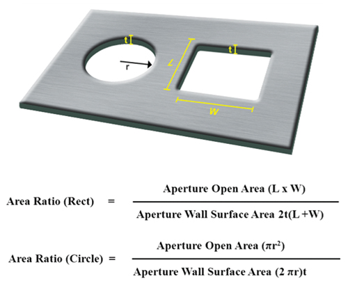
Figure 1. Area ratio calculation.
The factors that make up an aperture – stencil thickness, aperture diameter, width and length – all influence the subsequent area ratio. The effects can be observed with these two examples: A stencil of 100µm and a circular aperture of 240µm would result in an area ratio of 0.6. By changing the diameter to 20µm, the area ratio becomes 0.5. Needless to say, the act of calculating area ratio allows the engineer to quickly register an aperture dimension and produce an area ratio integer. The significance of this value is correlated to the transfer efficiency, or how much solder paste is expected to release from the aperture.
To aid the process engineer, IPC published a stencil guideline, IPC-7525B1, which recommends aperture area ratios in a range of 0.5 to 0.66 (material set dependent) to ensure a minimum 70 to 75% transfer efficiency and, therefore, an acceptable stencil printing process. FIGURE 2 illustrates the historical transfer efficiency curves that have been the accepted point of reference. As can be seen, the transfer efficiency of 70% falls off after area ratios of 0.66.
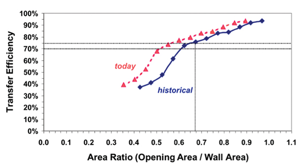
Figure 2. Transfer efficiency curves (historical and today).
Over the past few years, solder paste, stencil and capital equipment suppliers have invested resources into extending the process window, thus permitting smaller area ratios to achieve 70 to 75% transfer efficiency. These incremental developments are illustrated in Figure 2 (today curve). With careful selection of material sets and process setup, the smallest area ratio that can achieve 70 to 75% transfer efficiency has been extended to 0.5.
To illustrate the dilemma the automotive and industrial sectors face, the aperture range associated with the 0.4mm CSP device and calculated area ratios for both 100µm and 127µm stencil foil thicknesses are shown in TABLE 1. Although leading-edge print processes can achieve area ratios of 0.5, it is clear to see the 0.4mm CSP aperture range when combined with 127µm stencil thicknesses falls outside today’s capability.
Table 1. Area Ratio values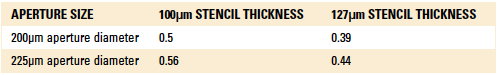
Within the consumer, computing and communications sectors, solutions such as nanocoatings 2-3, stencil manufacturing techniques4, stencil finish5-6 and activated squeegees7-8 have been investigated to break through the 0.5 area ratio barrier. From these documented innovations, the activated squeegee has shown the most capability. This device will be used throughout this investigation to establish if apertures ranging from 200µm to 225µm with associated area ratios of 0.39 to 0.44 can be printed.
Test vehicle. FIGURE 3 shows the test vehicle used through the investigation. This substrate contains standard device layouts that follow IPC recommendations. The outer dimensions are 150 x 150mm, with a thickness of 1mm. The substrate is fabricated from FR-4, and all pads are non-solder mask defined (NSMD).
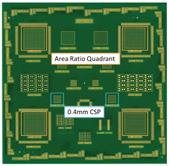
Figure 3. Test vehicle.
Two 0.4mm CSPs were used to measure the success of the investigation. The land patterns follow IPC recommendations. Aperture designs used for the investigation are shown in FIGURE 4. The associated area ratios are calculated assuming the stencil thickness is 127µm. As can be seen, the two designs aresignificantly below the current 0.5 limit.
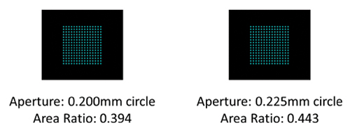
Figure 4. Aperture designs.
TABLE 2 shows the SIPOC diagram used throughout this investigation. The measurement tool used was a production solder paste inspection (SPI) machine with a micro-pad sensor. The measurement tool was set up to record solder paste height, area and volume for each printed deposit.
Gage R&R. Gage R&R was performed on the SPI tool to ensure the precision errors were acceptable. The Gage R&R test program consisted of a printed substrate, which was permitted to dry to ensure stability. This substrate was used for all Gage R&R trials. The Gage R&R test plan is outlined in FIGURE 5; each trial included six inspection cycles. Aperture sizes of 175µm, 200µm and 225µm were measured to understand the precision of the SPI machine. The design of the Gage R&R provides the study with 36 parts for each run, which generates 108 data points. Results are shown in FIGURES 6 and 7.
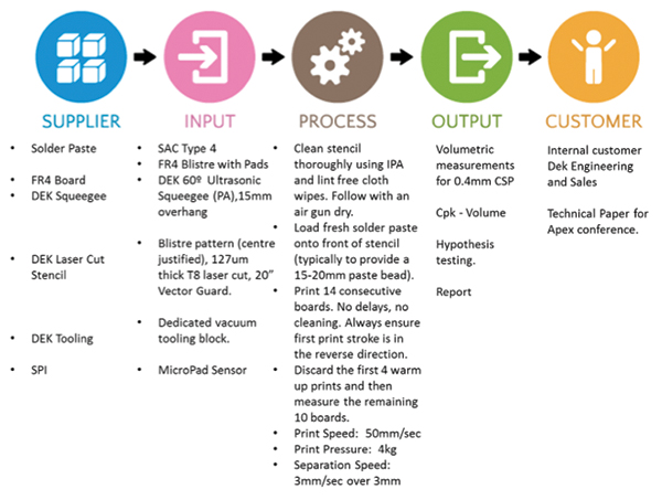
Figure 5. SIPOC diagram.
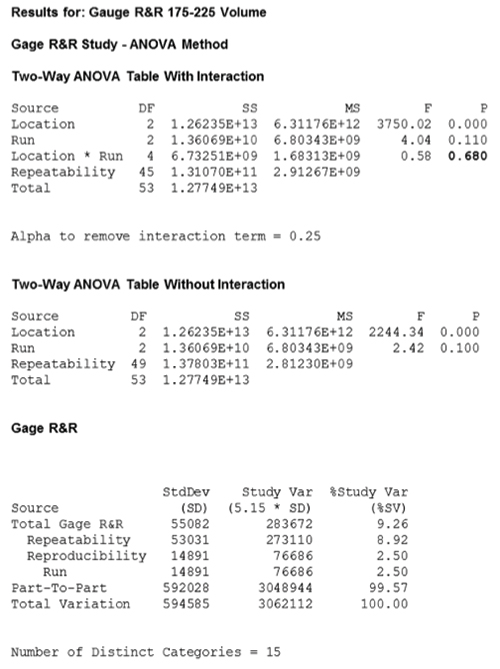
Figure 6. Gage R&R Anova results.
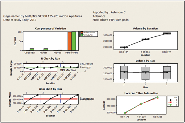
Figure 7. Gage R&R Anova plots.
The Anova results in Figures 6 and 7 show the p-value for “Run” is greater than 0.05 (alpha level 95%), indicating that this factor has no effect on the Gage R&R. Therefore, the only source that has an effect on the Gage R&R study is location. The % study variation figures for total Gage R&R, repeatability and reproducibility were below 10%, indicating the measurement tool has an acceptability rating of “Excellent”; therefore, this tool was used with confidence throughout the investigation.
Baseline results. Although area ratio calculations and historical references predict failure for the 200µm and 225µm aperture designs, the next stage was to test and benchmark the predicted output. Setups for these tests are outlined in the SIPOC.
The process capability for this benchmarking activity and subsequent test were measured against transfer efficiency (TE). TE is the ratio between the measured volume and the theoretical volume. (Note: Due to legacy, the results are reported in a decimalized percentage; i.e., 0.5 = 50%). A Cp and Cpk index of 1.33 or greater is required to verify a stable process output.)
FIGURES 8 and 9 show the process output achieved from the 200µm aperture design (area ratio = 0.394) with a standard print process setup. As is illustrated, the 200µm aperture’s process capability analysis indicates the process has a relatively low standard deviation (13%) but a mean volume of only 36%, producing a Cp of 1.1 and a Cpk of -0.67. This indicates the process is not capable.
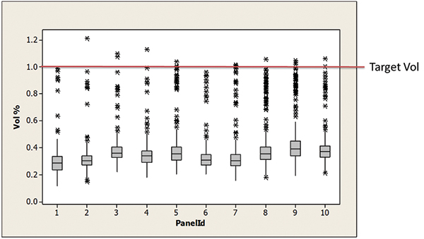
Figure 8. Boxplot 200µm aperture diameter standard process – activated Off.
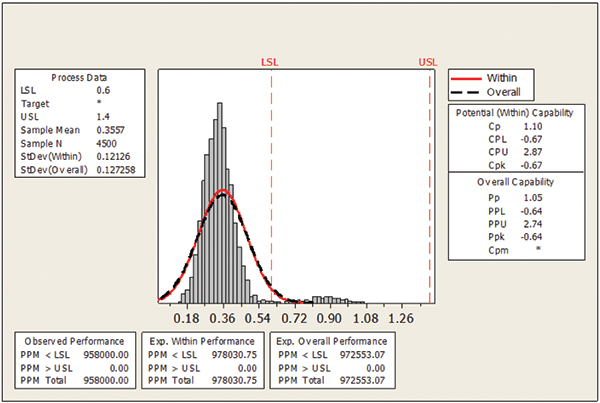
Figure 9. Process capability 200µm aperture diameter standard process – activated OFF.
FIGURES 10 and 11 show the process output achieved from the 225µm aperture design (area ratio = 0.443) with a standard print process setup. As can be seen, the 225µm aperture process capability analysis indicates the process has a relatively high standard deviation (31%), with a mean volume of only 59%, producing a Cp of 0.45 and a Cpk of -0.01. This suggests the process is not capable.
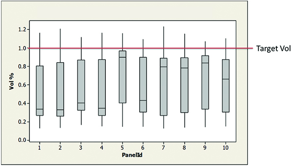
Figure 10. Boxplot 225µm aperture diameter standard process – activated OFF.
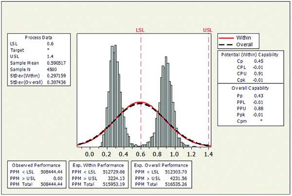
Figure 11. Process capability 225µm aperture diameter standard process – activated OFF.
Benchmark conclusions. The results from the baseline show that both aperture sizes deliver a process that falls outside the target Cp/Cpk. The 200µm aperture produces an output that has a low standard deviation (13%) but only manages a mean output of 36% volume. The 225µm aperture shows a tendency to improve the volumetric output, but the histogram shows that a bimodal output is present, which indicates poor process stability. Both experiments have failed to produce a satisfactory process and have therefore matched the predicted outcome of the area ratio model.
Design of Experiments
As concluded from the benchmark analysis, the aperture range required to print 0.4mm CSP devices is not capable with a standard process setup. A DoE technique was employed to determine the effect and interaction of both aperture size and squeegee type. Factors included were aperture size and squeegee type. The two-level full factorial experiment is illustrated in TABLE 3; each experiment was replicated 10 times. The DoE was conducted under the conditions outlined in the SIPOC.
Table 3. Design of Experiments
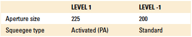
Analysis. FIGURE 12 outlines the DoE Anova table. As shown, the p-values of the terms are 0, which indicates that all terms are significant, and the R-Sq. value of 97.03% indicates that the majority of the resultant output is explained by the experiment.
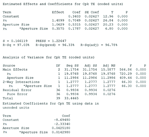
Figure 12. Design of experiments Anova.
FIGURE 13 clearly shows the impact of both factors: The Pareto chart indicates all features are important, with the activated squeegee (factor A) the most significant. FIGURE 14 illustrates the interaction plot, and the graph shows that even with the activated squeegee on, 200µm aperture did not meet the minimum 1.33 Cpk value; therefore, this aperture was discounted from the subsequent analysis.
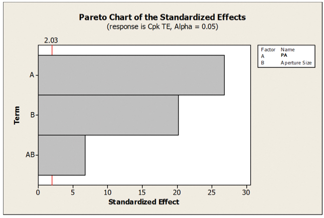
Figure 13. DoE Pareto chart
Figure 14. DoE interaction plot.
To better understand the impact of both factors, the coefficients derived from the Anova (Table 3) can be used to model the process; FIGURE 15 illustrates the derived mathematical model. This model also can be used to ascertain the effect on the process output as incremental changes are made to the aperture size, thus permitting the smallest capable aperture size to be discovered.

Figure 15. Mathematical model.
The software optimizer tool uses the mathematical model outlined in Figure 15 to graphically represent the changes in process output as the factors are modified. FIGURES 16 to 18 illustrate the output of this analysis. Figure 16 shows that with the activated squeegee OFF, the composite desirability yields a value of 0, thus indicating that no solution is possible independent of aperture size. Figure 17 illustrates that the model predicts the smallest aperture in which a Cpk of 1.33 is achievable is 217.5µm, whereas Figure 18 illustrates that the model predicts the 225µm aperture produces a Cpk value of 1.76.
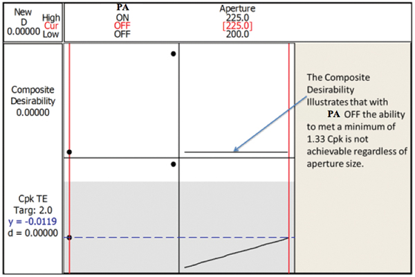
Figure 16. Predicted Cpk with no activated squeegee.
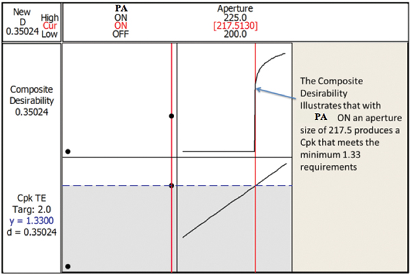
Figure 17. Predicted minimum aperture size with activated squeegee.
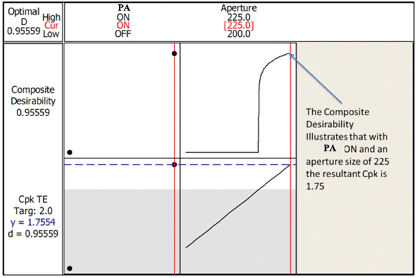
Figure 18. Predicted Cpk with largest aperture size with activated squeegee.
Apertures larger than 225µm are outside the experimental space and therefore not covered in this analysis. From an experienced-based viewpoint, larger apertures will tend to print much easier due to the larger corresponding area ratio. However, as aperture size increases, the interspace between deposits decreases. This decrease in interspace will tend to generate wet bridging between adjacent deposits, and, as a result, apertures of 225µm or less are recommended for a 0.4mm pitch CSP high-volume manufacturing assembly process.
Further Statistical Testing
To complete the statistical analysis, the following analysis investigated the 225µm aperture to establish if any statistical difference in transfer efficiency between activated and standard squeegee exists. FIGURES 19 and 20 show the non-normal distribution curves of the data; therefore, the Mood’s median test and test for equal variance were employed to perform the null hypothesis testing.
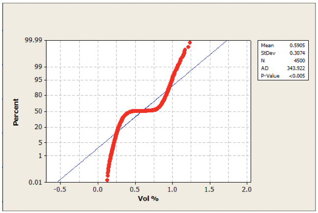
Figure 19. Probability plot 225µm activated OFF.
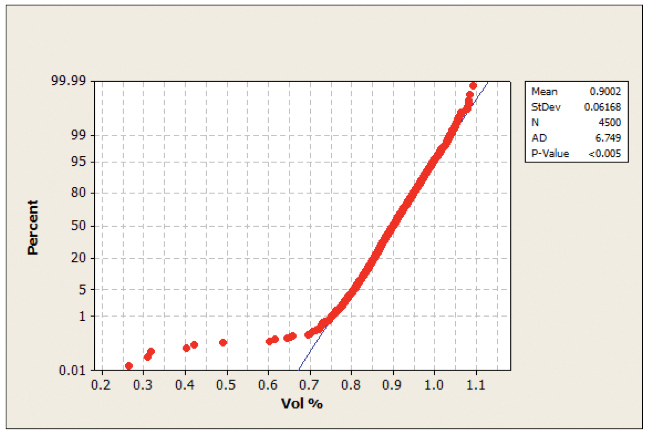
Figure 20. Probability plot 225µm activated ON.
FIGURE 21 illustrates the results from the Mood’s medians. The results show a p-value of 0, indicating that within a confidence level of 95% the medians are different. The confidence intervals (with 95% confidence) indicate that the transfer efficiency from an activated squeegee is improved between 25.8 and 46.8% with respect to a standard squeegee.
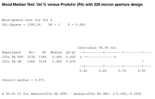
Figure 21. Moods median test 225µm aperture.
FIGURE 22 shows results from the test for equal variance and illustrates the standard deviation of each data set. As can be seen, the Levene’s test shows a value of zero, indicating that within the two subsets the standard deviations are different. The Bonferroni confidence intervals indicated the activated squeegee ON data set produces the lowest standard deviation.
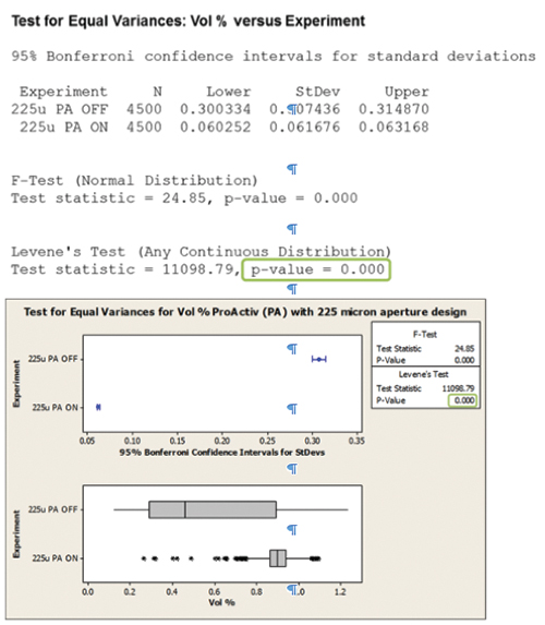
Figure 22. Test for equal variance 225µm aperture.
The Mood’s median and test for equal variance analysis shows that for the 255µm aperture there is a positive transformation in transfer efficiency between the standard and activated squeegee system.
Confirmation run. From the DoE and statistical testing, the 225µm aperture with activated squeegee demonstrated a capable process. The following discussion shows a confirmation run that used the 225µm aperture and activated squeegee in order to verify the finding. The confirmation run included a rebuild of the experiment setup as outlined in Figure 5.
FIGURE 23 illustrates the process output from the confirmation run. The resultant Cp/Cpk values were 2.31 and 1.73, both greater than the minimum required 1.33. This verifies the 225µm with activated squeegee is capable of printing 0.4mm CSP devices alongside 127µm stencil foils and other standard material sets used within the solder paste printing process.
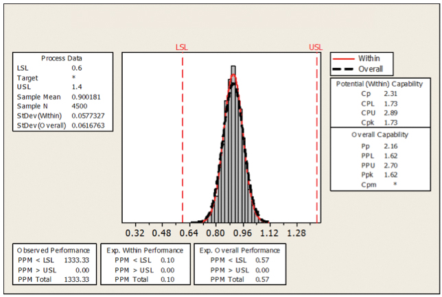
Figure 23. Rerun process capability.
Heterogeneous view. Testing so far has exclusively focused on implementing 0.4mm CSP technology for the 127µm stencil user. Obviously, for any solder paste printing solution to be accepted, its capability needs to cover a full range of deposits in different sizes and shapes. The following section reviews the investigation of the proposed 0.4mm CSP activated squeegee solution and the impact on a heterogeneous process.
The components included in this heterogeneous study were 0805s and 0.4mm quad flatpacks; aperture dimensions are outlined in TABLE 4. The process setup followed the SIPOC outlined in Figure 5, with the exception of the heterogeneous devices.
Table 4. Aperture Size for Heterogeneous Study
FIGURES 24 to 27 illustrate the normality testing of the 0805 and 0.4mm QFP with and without the activated squeegee. As illustrated, the p-values from the normality tests are less than 0.05, except for 0.4mm QFP activated squeegee OFF (Figure 26); for the sake of symmetry, all datasets are declared non-normally distributed.
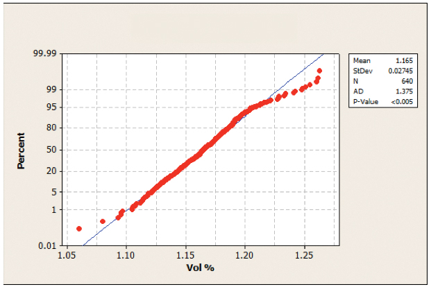
Figure 24. Normality test 0805 standard squeegee.
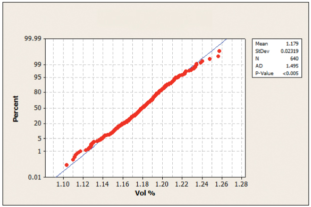
Figure 25. Normality test 0805 activated squeegee.
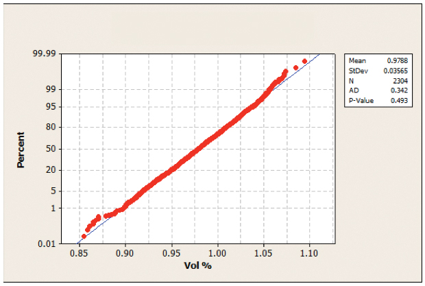
Figure 26. Normality test 0.4mm QFP standard squeegee.
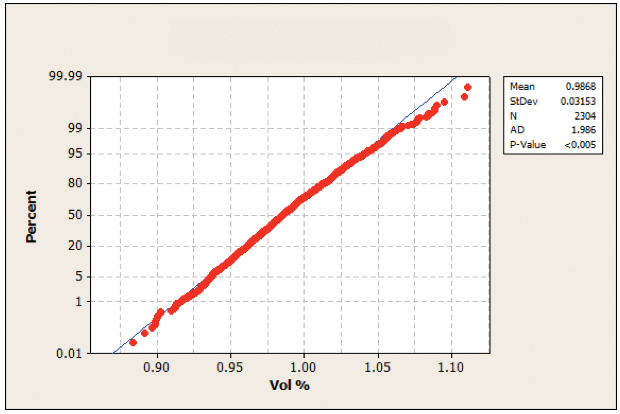
Figure 27. Normality test 0.4mm QFP ultrasonic squeegee.
To understand if the activated squeegee yields an impact on the heterogeneous aspect of solder paste printing, the data were analyzed using a Mood’s median, test for equal variance and process capability study.
FIGURES 28 to 31 illustrate the analysis of the 0805 and 0.4mm QFP devices. The Mood’s median analysis displays a p-value of zero for both the 0805 and 0.4mm QFP device types. This indicates that, with 95% confidence, the medians of the subgroups (activated squeegee ON/OFF) are dissimilar. The test for equal variance displays a p-value (Levene’s Test) of zero for both the 0805 and 0.4mm QFP package types. This indicates that, with 95% confidence, the variation (standard deviation) of the subgroups (activated squeegee ON/OFF) is dissimilar.
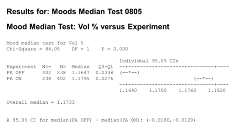
Figure 28. Moods Median test 0805.
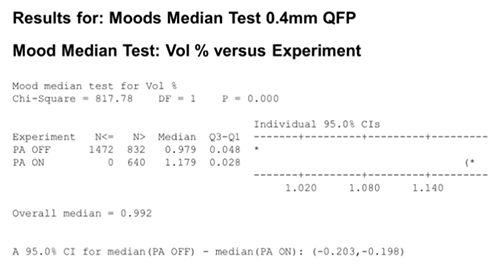
Figure 29. Moods Median test 0.4mm QFP.
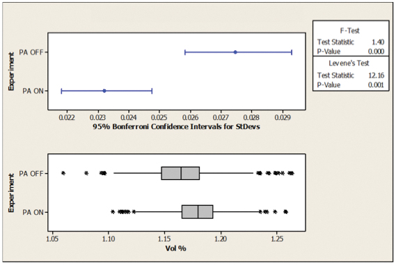
Figure 30. Test for equal variance0805.
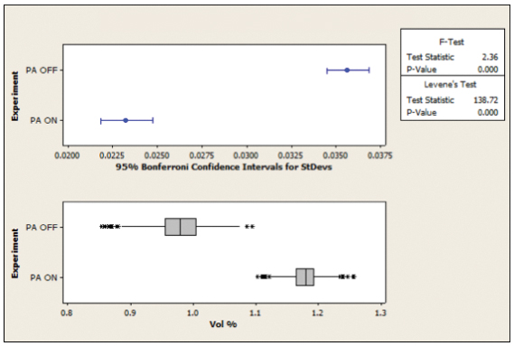
Figure 31. Test for equal variance 0.4mm QFP.
The following analysis investigated and answers whether differences between the subsets affect the process output.
FIGURES 32 to 35 illustrate the process capability output for the 0805 and 0.4mm QFP packages. Each package type was analyzed under the condition of activated squeegee ON/OFF.
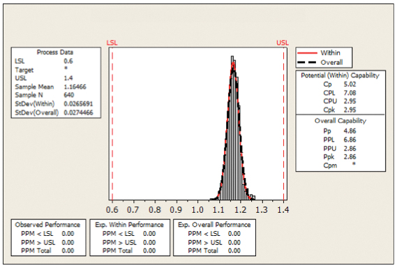
Figure 32. Process capability 0805 standard squeegee.
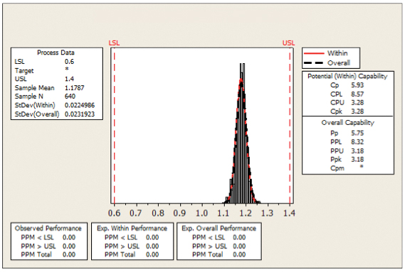
Figure 33. Process capability 0805 activated squeegee
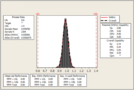
Figure 34. Process capability 0.4mm QFP standard squeegee
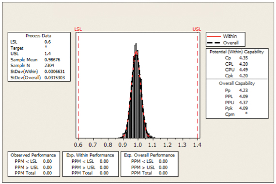
Figure 35. Process capability 0.4mm QFPactivated squeegee.
The process capability curves in Figures 32 and 34 show the output from a standard system (activated squeegee OFF). The results show both devices within the required ≥1.33 Cpk value, an expected outcome, as both devices are representative of today’s standard assembly processes.
The process capability curves in Figures 33 and 35 show the output from an activated squeegee system. Here, the Cpk index value is greater when the activated condition is ON, indicating that the addition of an ultrasonic device has process capability benefits to the larger footprint devices. For reference, the results for both conditions are presented in TABLE 5.
Table 5. Cpk Values for 0805 and 0.4mm QFP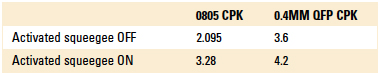
Conclusions
The purpose of this investigation was to determine whether 0.4mm CSP devices can be effectively printed within automotive and industrial assembly environments. As considered throughout this work, the issue of printing 0.4mm CSP-compatible apertures through the established 127µm stencil foil thickness leads to an infringement of industry-recognized area ratio rules. Therefore, this investigation focused around the possibility of breaking these established area ratios with no detrimental effect on standard depositions.
The findings from this investigation are:
- The activated squeegee extended the print process window to include area ratios ≥ 0.45. This permits 225µm apertures to be printed using 127µm stencil foils.
- The 200µm diameter apertures were outside the activated squeegee’s capability. Therefore, the ability to print area ratios below 0.4 using this aperture dimension is still an unknown.
- The ability to print 225µm diameter apertures using 127µm stencil foil thicknesses gives the automotive and industrial sectors the possibility of printing solder paste deposits for the 0.4mm CSP.
- The inclusion of an activated squeegee does not adversely affect paste deposition of larger-footprint devices.
- Therefore, the ability to print 0.4mm CSP-compatible apertures using incumbent material sets is possible when activated squeegee technology is employed. CA
References
1. IPC-7525B, Stencil Design Guidelines, 2012.
2. Läntzsch, “Nano Coated SMT Stencil with Anti-adhesion Effect,” epp-online.de, September 2008.
3. Manessis, R. Patzelt, A. Ostmann, R. Aschenbrenner, H. Reichl, A. Axmann and G. Kleemann, “Evaluation of Innovative Nano-Coated Stencils in Ultra-Fine Pitch Flip Chip Bumping Processes,” IMAPS 41st International Symposium on Microelectronics, November 2008.
4. Läntzsch and G. Kleeman, “Challenges for Step Stencil with Design Guidelines for Solder Paste Printing,” IPC Apex Expo, February 2012.
5. Burkhalter, E. Leak, C. Shea, R. Tripp and G. Wade, “Transfer Efficiencies in Stencil Printing” SMT, May 2007.
6. Fleck and P. Chouta, “A New Dimension in Stencil Print Optimization,” SMTA International, September 2002.
7. Ashmore and M. Whitmore, “The Development of a 0.3mm Pitch CSP Assembly Process Using Standard Materials,” SMTA International, October 2011.
8. Ashmore and M. Whitmore, “A Revolutionary Printing Solution for Heterogeneous Surface Mount Assembly,” IPC Apex Expo, April 2011.
Ed.: This article was first published at IPC Apex Expo in March 2014 and is published here with permission of the authors.
is global applied process engineering manager and is future technologies manager at ASM Assembly Systems, Printing Solutions Division (asmpt.com); clive.ashmore@asmpt.com.


Press Releases
- Seika Machinery’s SMI 2026 Webinar Series Continues with Focus on PCB Cleaning Before Solder Paste Printing
- Forwessun Expands Testing Capabilities through Strategic TRI Alliance
- Federal Electronics Expands Advanced Manufacturing Capabilities to Support Military and Aerospace Cable Assembly and Wire Harness Programs
- Altus Continues Irish Growth with Expansion of Engineering Team